Manufacturing method of conductive interconnection line

A technology of conductive interconnection and manufacturing method, applied in the field of manufacture of conductive interconnection lines, to achieve the effects of avoiding bridging, easy implementation, and improving performance and yield

Pending Publication Date: 2020-05-29
NEXCHIP SEMICON CO LTD
View PDF0 Cites 0 Cited by
  • Summary
  • Abstract
  • Description
  • Claims
  • Application Information

AI Technical Summary

Problems solved by technology

[0008] The purpose of the present invention is to provide a method of manufacturing conductive interconnection wires to solve the problem of bridging between conductive interconnection wires

Method used


Image

  • Manufacturing method of conductive interconnection line
  • Manufacturing method of conductive interconnection line
  • Manufacturing method of conductive interconnection line

Examples


Embodiment Construction

[0038] The technical solutions proposed by the present invention will be described in further detail below in conjunction with the accompanying drawings and specific embodiments. The advantages and features of the present invention will become clearer from the following description. It should be noted that all the drawings are in a very simplified form and use imprecise scales, and are only used to facilitate and clearly assist the purpose of illustrating the embodiments of the present invention. The meaning of "and / or" in this article is to choose one or both.

[0039] Please refer to figure 2 , the invention provides a method for manufacturing a conductive interconnection wire, comprising the following steps:

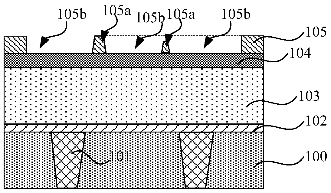
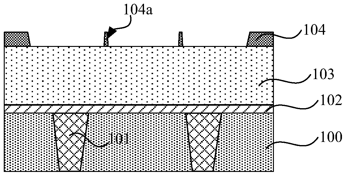
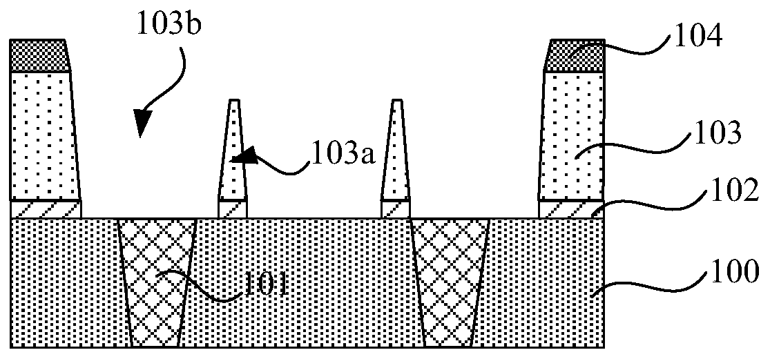
[0040] S1, providing a substrate, a first interlayer dielectric layer is formed on the substrate, at least one conductive plug is embedded in the first interlayer dielectric layer, and the first interlayer dielectric layer is covered with the first interlayer dielect...


PUM


Abstract

The invention provides a manufacturing method of a conductive interconnection line. The method comprises the steps: forming a second interlayer dielectric layer and a patterned photoresist layer on afirst interlayer dielectric layer with a conductive plug, taking the patterned photoresist layer as a mask, and carrying out etching to remove a part of the second interlayer dielectric layer at a certain thickness so as to form a corresponding first groove; then, removing the patterned photoresist layer, and forming a hard mask layer used for filling the first groove, wherein the hard mask layeris embedded in the second interlayer dielectric layer and can define interval areas between the conductive interconnection lines; then, etching the second interlayer dielectric layer by taking the hard mask layer as a mask to form a second groove; and finally, forming the conductive interconnection line which is filled in the second groove and is in contact with a top of the corresponding conductive plug. According to the scheme, a width of the gap between the formed conductive interconnection lines can be accurately and effectively controlled through the hard mask layer, and a problem of bridging of the conductive interconnection lines is avoided.

Description

technical field [0001] The invention relates to the technical field of integrated circuit manufacturing, in particular to a method for manufacturing conductive interconnection lines. Background technique [0002] In the back-end process (Back End of Line, BEOL) of semiconductor devices, it is necessary to form several layers of metal interconnection lines and contact plugs between metal interconnection lines of different layers on the semiconductor device layer, so that the semiconductor The electrodes of the device are drawn out. With the continuous development of semiconductor technology, the critical dimension (CD) of semiconductor devices continues to shrink, the metal interconnection lines become thinner, and the gaps between the metal interconnection lines become smaller and smaller. When the photoresist used to define the metal interconnection line is exposed, if the photoresist line is relatively thin and the area of ​​the light-transmitting area around it is relati...

Claims


Application Information

Patent Timeline
IPC IPC(8): H01L21/768H01L21/311H01L23/522
CPCH01L21/76816H01L21/76877H01L21/31144H01L23/5226
Inventor 张傲峰李建财陈世昌王建智
Owner NEXCHIP SEMICON CO LTD
Why Eureka
Try Eureka