Semiconductor device, manufacturing method thereof and electronic device

A manufacturing method and semiconductor technology, applied in semiconductor/solid-state device manufacturing, circuits, transistors, etc., can solve problems such as bridging, and achieve the effect of reducing RC delay, improving performance and reliability, and avoiding bridging

Active Publication Date: 2017-11-21
SEMICON MFG INT (SHANGHAI) CORP +1
View PDF4 Cites 0 Cited by
  • Summary
  • Abstract
  • Description
  • Claims
  • Application Information

AI Technical Summary

Problems solved by technology

[0003] Although embedded silicon germanium technology has a certain effect on improving the performance of PMOS devices, there are still many problems in conventional embedded silicon germanium technology, suc

Method used


Image

  • Semiconductor device, manufacturing method thereof and electronic device
  • Semiconductor device, manufacturing method thereof and electronic device
  • Semiconductor device, manufacturing method thereof and electronic device

Examples


Embodiment 1

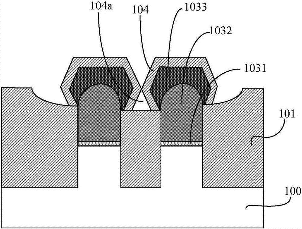
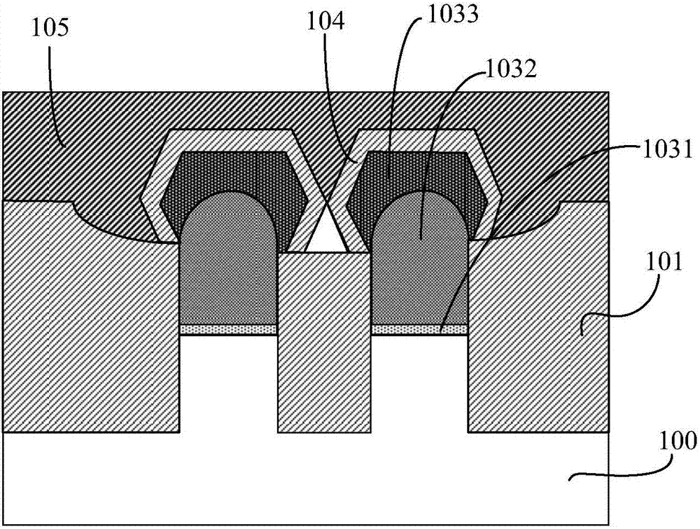
[0058] Below, refer to Figure 1A to Figure 1E The detailed steps of an exemplary method of the semiconductor device manufacturing method proposed by the embodiment of the present invention will be described. Among them, 1A to Figure 1E It is a cross-sectional view of a structure formed in related steps of a method for manufacturing a semiconductor device according to an embodiment of the present invention.

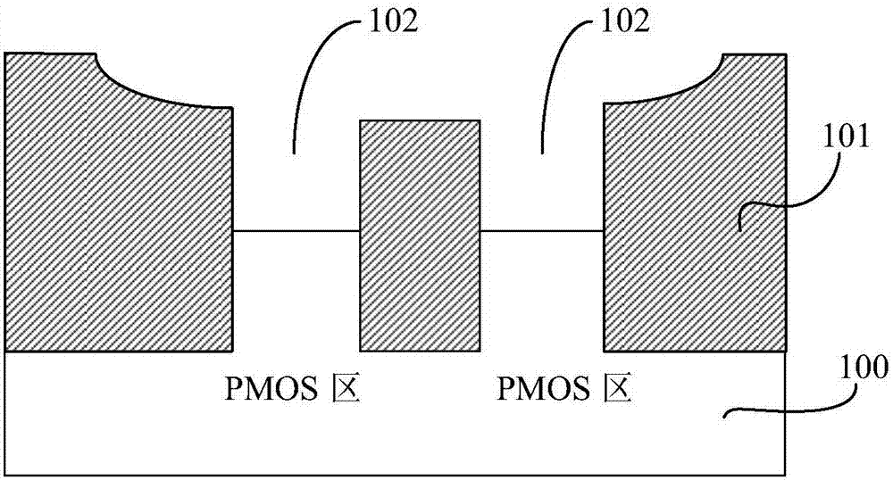
[0059] First, if Figure 1A As shown, a semiconductor substrate 100 is provided. The semiconductor substrate 100 includes at least two adjacent PMOS regions. A plurality of isolation structures 101 are formed in the semiconductor substrate 100 to define each of the PMOS regions. Grooves 102 are formed between the isolation structures 101 in adjacent PMOS regions.

[0060] The constituent materials of the semiconductor substrate 100 can be undoped single crystal silicon, single crystal silicon doped with impurities, silicon on insulator (SOI), silicon on insulator (SSO...

Embodiment 2

[0098] The present invention also provides a semiconductor device fabricated by the aforementioned method, and the semiconductor device may be a static random access memory (SRAM) or the like.

[0099] As an example, refer to Figure 1E The structure of the semiconductor device of the present invention is described in detail.

[0100] like Figure 1E As shown, the semiconductor device of the present invention includes a semiconductor substrate 100. 11. A semiconductor device is characterized in that it includes a semiconductor substrate 100, and the semiconductor substrate 100 includes at least two adjacent PMOS regions. A plurality of isolation structures 101 are formed in the semiconductor substrate 100 to define each of the PMOS regions, and grooves 102 are formed between the isolation structures 101 in adjacent PMOS regions.

[0101] The constituent materials of the semiconductor substrate 100 can be undoped single crystal silicon, single crystal silicon doped with impur...

Embodiment 3

[0126] An embodiment of the present invention provides an electronic device, which includes an electronic component and a semiconductor device electrically connected to the electronic component. Wherein, the semiconductor device includes the semiconductor device manufactured according to the method for manufacturing a semiconductor device described in Embodiment 1, or includes the semiconductor device described in Embodiment 2.

[0127]The electronic device of this embodiment can be any electronic product or equipment such as mobile phone, tablet computer, notebook computer, netbook, game console, TV set, VCD, DVD, navigator, camera, video recorder, voice recorder, MP3, MP4, PSP, etc. , can also be any intermediate product including the frequency division circuit. Wherein, the electronic component may be any feasible component, which is not limited here.

[0128] The electronic device according to the embodiment of the present invention has better performance due to the use o...


PUM

PropertyMeasurementUnit
Thicknessaaaaaaaaaa
Thicknessaaaaaaaaaa

Abstract

The invention provides a semiconductor device, a manufacturing method thereof and an electronic device, and relates to the technical field of semiconductors. The method includes the steps of providing a semiconductor substrate including at least two adjacent PMOS regions, recesses being formed between isolation structures in the adjacent PMOS regions; forming seed layers on the semiconductor substrate at the bottoms of the recesses; forming bulk germanium-silicon layers on the seed layers; forming cap germanium-silicon layers on the bulk germanium-silicon layers, the cap germanium-silicon layers having a [sigma]-shaped structure; forming a conformal covering layer on the exposed peripheral surface of each cap germanium-silicon layer, and bringing part of the covering layers in the adjacent PMOS regions in contact to form an air gap; forming a dielectric layer on the isolation structures and the covering layers; and etching back part of the dielectric layer and part of the covering layers to expose the top surfaces of the cap germanium-silicon layers. The manufacturing method of the invention can reduce the RC delay of the device and avoid bridging between metal silicides formed on the embedded germanium-silicon top surface.

Description

technical field [0001] The present invention relates to the technical field of semiconductors, in particular to a semiconductor device, a manufacturing method thereof, and an electronic device. Background technique [0002] In order to improve the mobility of carriers in the channel of PMOS devices, the technology of making grooves in the part of PMOS devices where the source / drain regions will be formed and epitaxially embedded silicon germanium has become a hot spot of widespread concern. For the semiconductor manufacturing process of 45nm and below nodes, due to the scaling down of the device size, the length of the device channel is also shortened accordingly. The indented Σ-shaped groove in the channel direction can effectively shorten the length of the device channel and meet the proportional reduction requirements of the device size; at the same time, this Σ-shaped groove has the characteristics of a large undercut under the gate spacer, thus , the embedded silicon g...

Claims


Application Information

Patent Timeline
IPC IPC(8): H01L27/088H01L21/8234
CPCH01L21/823418H01L21/823481H01L27/088
Inventor 林静
Owner SEMICON MFG INT (SHANGHAI) CORP
Why Eureka
Try Eureka