White light interference measurement device and method based on sample space structure illumination

A technology of white light interference and spatial structure, applied in the direction of measuring devices, optical devices, image data processing, etc., can solve the problems of inapplicability, poor applicability, long measurement time, etc., and achieve suppression of signal interference, wide application range, The effect of high signal-to-noise ratio

Active Publication Date: 2020-06-02
INST OF MACHINERY MFG TECH CHINA ACAD OF ENG PHYSICS
View PDF8 Cites 6 Cited by
  • Summary
  • Abstract
  • Description
  • Claims
  • Application Information

AI Technical Summary

Problems solved by technology

Microprobe scanning method ("B.Ju, Y.Chen, W.Zhang, et al.Note: long range and accurate measurement of deep trenchmicrostructures by a specialized scanning tunneling microscope, Rev.Scie.Instrum.2012,83:056106 ") There is no need to consider the multiple reflection interference of optical measurement methods, but limited by the length of the probe, contact force, and scanning speed, it can only measure microstructures with a depth of tens of microns, and it will scratch the surface of the sample, and the measurement time is long
The improved interferometric method is to treat the sample surface or plan the measurement process in the existing interference optical path, such as: coating the refractive index matching liquid on the sample surface to reduce the wavefront gradient ("D.Purcell, A.Suratkar, A.Davies , etal.Interferometric technique for faceted microstructure metrology using anindex matching liquid.Appl.Opt.2010,49:732"), but it can only be used for the detection of transmissive samples; establish multiple reflection models, plan from the bottom of the groove to the higher Low scanning range (“F. Fang, Z. Zeng, X. Zhang, e

Method used


Image

  • White light interference measurement device and method based on sample space structure illumination
  • White light interference measurement device and method based on sample space structure illumination
  • White light interference measurement device and method based on sample space structure illumination

Examples


Example Embodiment

[0036] Example 1:

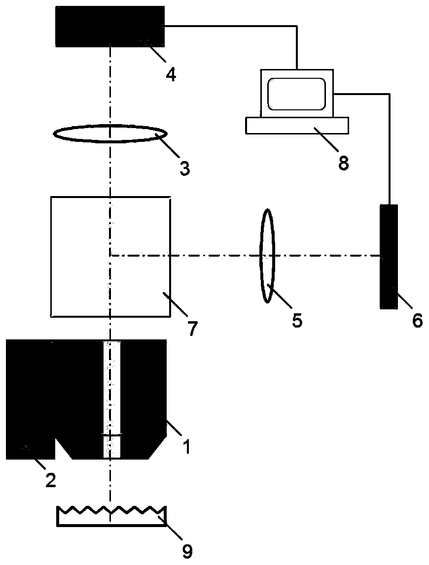
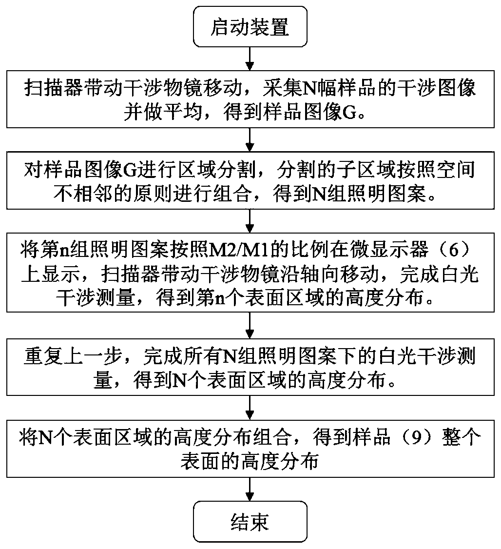
[0037] Such as figure 1 As shown, a white light interferometry device illuminated according to the sample space structure includes a coherent scanning interferometric system and a patterned illumination system;

[0038] The coherent scanning interference system is composed of an interference objective lens 1, a scanner 2, a tube lens 3 and an image sensor 4; the interference objective lens 1 is mounted on the scanner 2; the pattern illumination system is composed of an interference objective lens 1, a projection lens 5 and The microdisplay 6 is composed of the coherent scanning interference system and the patterned illumination system using the same interference objective lens 1, the coherent scanning interference system and the patterned illumination system are combined through a beam splitter 7 in a posture where the optical axes are perpendicular to each other, the image sensor 4 is conjugated with the object plane of the interference objective lens 1, and th...


PUM


Abstract

The invention discloses a white light interference measurement device and method based on sample space structure illumination. A micro-display is added to an illumination system, and different space patterns can be projected to the surface of a sample; during measurement, a measurement area of the sample is divided according to an acquired sample image in combination with characteristics of the sample to form different illumination patterns; the illumination patterns are input into the micro-display, and asynchronous spatial illumination and white light interference measurement are carried outon adjacent areas, so as to avoid coherent interference signal interference caused by multiple reflections between adjacent points; and then, the plurality of groups of measured surface height distributions are combined to obtain the height distribution of the whole surface. Interference between adjacent points during white light interference measurement of samples such as a micro-groove array issuppressed by adopting a spatial pattern illumination method, and the samples can be quickly detected in a nondestructive manner.

Description

technical field [0001] The invention relates to the field of micro-nano measurement, in particular to a white light interferometric measurement device and method based on sample space structure illumination. Background technique [0002] White light interferometry can measure the roughness and microstructure profile of the surface, and the precision can reach the micro-nano level, which is a key technology in the field of micro-nano measurement. White light interference scans the sample surface vertically to obtain coherent interference signals at every point on the surface. The contrast of the coherent interference signal is maximized when the sample surface is at the same optical path as the reference mirror. Therefore, the height information of the point on the sample can be determined by analyzing the coherent interference signal of each point. Because white light interference analyzes the coherent interference signal at each point, it has high spatial resolution and h...

Claims


Application Information

Patent Timeline
IPC IPC(8): G01B9/02G01B11/25G06T7/11
CPCG01B9/02083G01B9/02085G01B9/0209G01B11/2441G01B11/254G06T7/11
Inventor 刘乾李璐璐张辉黄小津
Owner INST OF MACHINERY MFG TECH CHINA ACAD OF ENG PHYSICS
Why Eureka
Try Eureka