Array substrate, display panel and liquid crystal display device
A technology for liquid crystal display devices and array substrates, which is applied in the fields of display panels, liquid crystal display devices, and array substrates, and can solve problems such as image retention, and achieve the effects of improving stability, good user experience, and improving image retention
- Summary
- Abstract
- Description
- Claims
- Application Information
AI Technical Summary
Problems solved by technology
Method used
Image
Examples
Embodiment 1
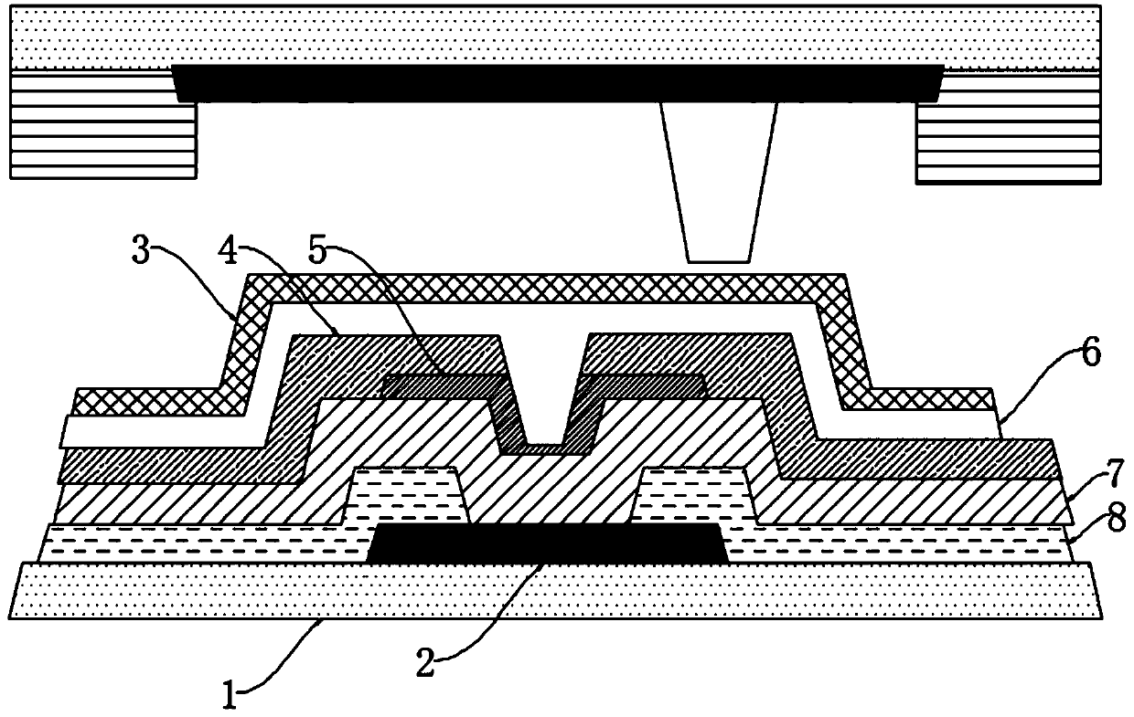
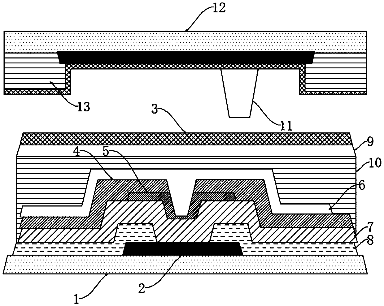
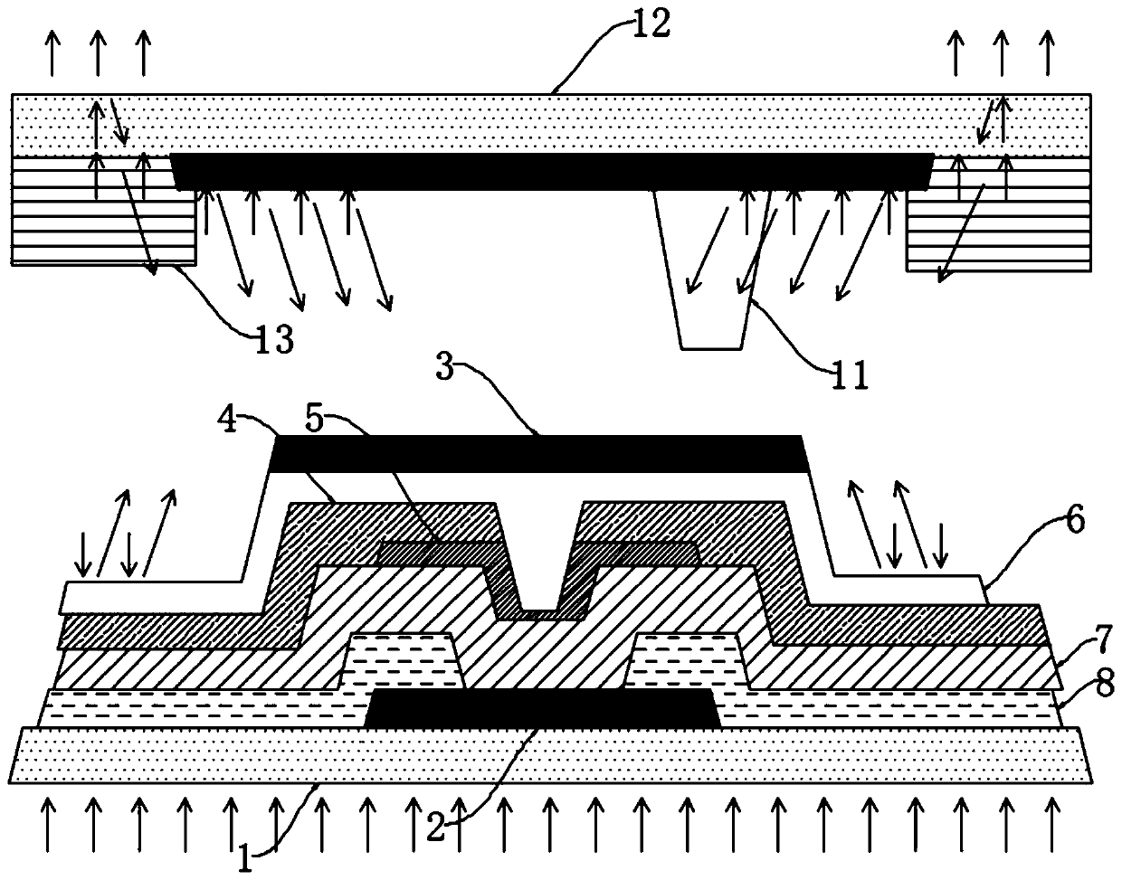
[0039] see Figure 7 , Figure 7 It is a schematic diagram of the spatial light path entering the channel region of the array substrate. exist Figure 7 After the light shown below enters, the cell gap of the display panel (such as Figure 7 The space between the black matrix layer above the first passivation layer 6 and below the second substrate 12) has light entering, although the channel region can be affected by the first light shielding layer 2 and the black matrix layer below the second substrate 12. For protection, but the light will be diffusely reflected in the cell, and the diffusely reflected light can still enter the channel area (the area shown by the inverted trapezoid in the center of the figure), such as Figure 7 As shown, the light entering the channel region increases the photo-generated carriers in the channel region of the TFT device, which in turn leads to an increase in the leakage current. Working, abnormally working liquid crystals may often cause...
Embodiment 2
[0050] Based on the same inventive concept as Embodiment 1, this embodiment provides a display panel, the display panel includes an array substrate of any structural form in Embodiment 1, and the specific structure of the array substrate is as described in Embodiment 1, This embodiment will not be repeated here, such as Figure 1-7 As shown, the display panel may further include a second substrate 12 disposed above the protective layer 3, and a second color resist layer 13 is disposed under the second substrate 12. In this embodiment, the second color resist layer 13 may be red At least one color resist among color resists, green resists, or blue resists. When this embodiment is implemented, the second color resist layer 13 on the left can be green resists, red resists, or blue resists, and the second color resist on the right The resist layer 13 may be a red resist or a green resist or a blue group. In specific implementation, the second substrate 12 can often be a CF (color...
Embodiment 3
[0052] Based on the same inventive concept as the first embodiment, this embodiment provides a liquid crystal display device, the liquid crystal display device includes the display panel in the second embodiment or the array substrate in the first embodiment, and in a specific application, the liquid crystal display device The device can be a display screen of a smartphone, tablet computer, notebook computer, smart bracelet, smart watch, smart glasses, smart helmet, desktop computer, smart TV or digital camera, etc. on electronic devices.
PUM
 Abstract
Description
Claims
Application Information


