
Preparation method for near-infrared quantum clipping film of nano pyramid light trapping structure

A light-trapping structure and quantum tailoring technology, applied in the field of solar cells, can solve the problems of serious powder scattering, poor transparency, and restrictions on the practical application of solar cells, so as to improve conversion efficiency, reduce short-circuit current, and improve low working efficiency.

Active Publication Date: 2013-11-06
BEIJING UNIV OF TECH
View PDF3 Cites 0 Cited by
  • Summary
  • Abstract
  • Description
  • Claims
  • Application Information

AI Technical Summary

Problems solved by technology

But now people's research on down-conversion materials is still mainly in powder, because the powder has serious scattering of incident light and poor transparency, which limits its practical application in solar cells.

Method used


Image

  • Preparation method for near-infrared quantum clipping film of nano pyramid light trapping structure
  • Preparation method for near-infrared quantum clipping film of nano pyramid light trapping structure
  • Preparation method for near-infrared quantum clipping film of nano pyramid light trapping structure

Examples


Embodiment 1

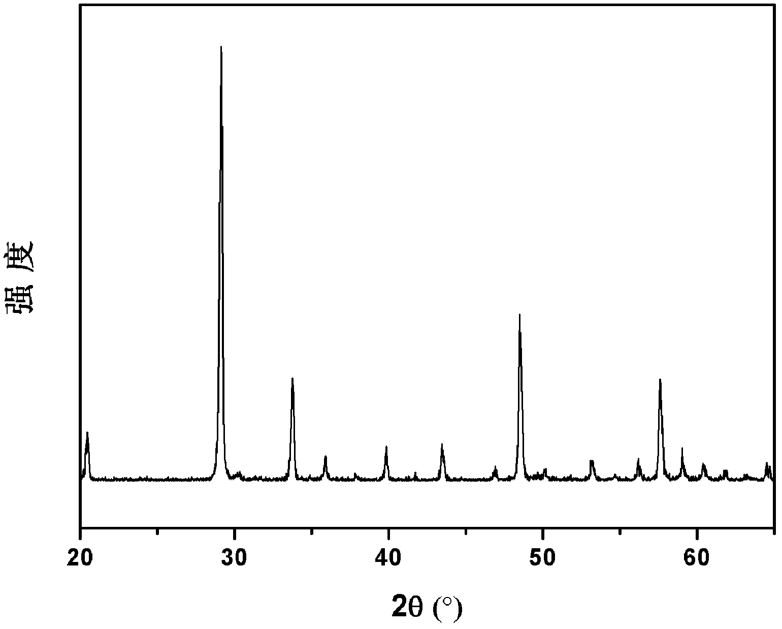
[0027] (1) in Y 2 o 3 The powder is mixed with an appropriate amount of Bi 2 o 3 and Yb 2 o 3 powder, where Bi 2 o 3 Powder mole fraction is 0.5%, Yb 2 o 3 The mole fraction of the powder is 2.5%, then ball milled and mixed, and dried at 80°C. Place the dried powder in a grinding tool and press it at 15MPa for 10 minutes to obtain a disc with a diameter of 2cm and a thickness of 5mm. The disc is calcined at 1100°C for 24h to make a ceramic target. The XRD pattern of its ceramic target material (see figure 1 ) exactly matches Y 2 o 3 PDF 41-1105 Diffraction Standard Spectrum.

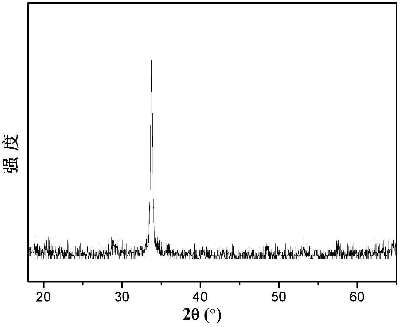
[0028] (2) Y made by step (1) 2 o 3 :Bi, Yb ceramic target, using laser pulse deposition method, using silicon wafer as substrate, passing O with a purity of 99.999% 2 , the substrate temperature is 700°C, the target-base distance is 8cm, the working pressure is 5Pa, the laser energy is 350mJ / pulse, and the deposition time is 60min. get pure phase Y 2 o 3 film, its XRD pattern is shown ...

Embodiment 2

[0030] in Y 2 o 3 The powder is mixed with an appropriate amount of Bi 2 o 3 and Yb 2 o 3 of powder, where Bi 2 o 3 Powder mole fraction is 1%, Yb 2 o 3 The mole fraction of the powder is 0.5%, then ball milled and mixed, and dried at 80°C. Place the dried powder in a grinding tool and press at 15MPa for 10 minutes to obtain a disc with a diameter of 2cm and a thickness of 5mm. The disc is calcined at 1200°C for 20h to make a ceramic target. The XRD pattern of its ceramic target is completely consistent with Y 2 o 3 PDF41-1105 Diffraction Standard Spectrum.

[0031] (2) Y made by step (1) 2 o 3 :Bi, Yb ceramic target, using laser pulse deposition method, using silicon wafer as substrate, passing O with a purity of 99.999% 2 , the substrate temperature is 800°C, the target-base distance is 5cm, the working pressure is 3Pa, the laser energy is 400mJ / pulse, and the deposition time is 60min. The XRD spectrum of the resulting film is shown in Figure 8 . Find that ...

Embodiment 3

[0033] (1) in Y 2 o 3 Add Bi to the powder 2 o 3 Powder and Yb 2 o 3 of powder, where Bi 2 o 3 Powder mole fraction is 0.25%, Yb 2 o 3 The molar fraction of the powder is 5%, then ball milled and mixed, and dried at 80°C. Place the dried powder in a grinding tool and press at 15MPa for 10 minutes to obtain a disc with a diameter of 2cm and a thickness of 5mm. The disc is calcined at 1300°C for 20h to make a ceramic target.

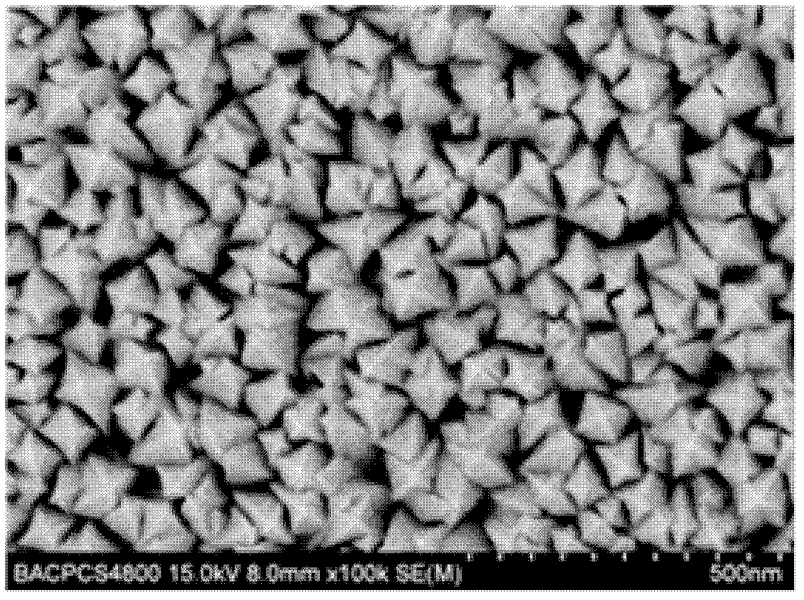
[0034] (2) Y made by step (1) 2 o 3 :Bi, Yb ceramic target, using laser pulse deposition method, using silicon wafer as substrate, passing O with a purity of 99.999% 2 , the substrate temperature is 500°C, the target-base distance is 6cm, the working pressure is 7Pa, the laser energy is 200mJ / pulse, and the deposition time is 60min. Its surface has a nano-pyramid structure (such as Figure 11 ), this film with a nano-pyramid structure has a good anti-reflection and light-trapping effect. Use FLS920 fluorescence spectrometer to measure the emi...


PUM

PropertyMeasurementUnit
diameteraaaaaaaaaa
thicknessaaaaaaaaaa
reflectanceaaaaaaaaaa

Abstract

A preparation method for a near-infrared quantum clipping film of a nano pyramid light trapping structure belongs to the field of solar cells. The film is capable of reducing reverse trapping light and clipping near-infrared quantum. The film is made of Y2O3, Bi2O3 and Yb2O3, wherein the molar fraction of the Bi2O3 is 0.25-1%; and the molar fraction of the Yb2O3 is 0.5-5%. The preparation method comprises the steps of adding Bi2O3 powder and Yb2O3 powder in Y2O3 powder, ball-milling and mixing the powder, and then drying the powder at 80 DEG C; arranging the dried powder in an abrasive tool, pressing the powder for 10min at 15MPa to obtain a wafer, of which the diameter is 2cm and the thickness is 5mm, and burning the wafer for 20-24h at 1,100-1,300 DEG C to prepare a ceramic target; and introducing O2 by laser pulse deposition method and taking a silicon wafer as a substrate, wherein the substrate temperature is 500-800 DEG C, the target distance is 6-8cm, the work air pressure is 3-7Pa, and the laser energy is 200-400mJ / pulse. The film has better effect for reducing reverse trapping light from ultraviolet light to near-infrared light; under the excitation of the ultraviolet light, the high-efficiency near-infrared quantum clipping switching light can be realized; the reflection and thermalization effects on the surface of silicon solar cell are expected to be reduced; and the photoelectric conversion efficiency of the cell is improved.

Description

technical field [0001] The invention belongs to the field of solar cells, and in particular relates to a rare earth-doped thin film with a nano-pyramid light-trapping structure and a high-efficiency near-infrared quantum tailoring down-conversion luminescence capable of improving the efficiency of a silicon solar cell and a preparation process thereof. Background technique [0002] Photovoltaic power generation of solar cells is a clean and safe renewable energy source. Due to the limitations of principles, structures, and materials, the improvement of the efficiency of solar cells with traditional structures is facing major challenges. Since silicon solar cells will be dominant for a long time, it is of great significance to carry out research on improving the light utilization efficiency of silicon solar cells. Silicon has a high refractive index. Generally, the reflectivity of sunlight on the surface of bare silicon reaches more than 30%, so that a large amount of light f...

Claims


Application Information

Patent Timeline
Patent Type & Authority Patents(China)
IPC IPC(8): H01L31/18H01L31/0216H01L31/055B82Y20/00
CPCY02E10/50Y02E10/52Y02P70/50
Inventor 王如志曲铭浩严辉张铭王波宋雪梅朱满康侯育冬刘晶冰汪浩
Owner BEIJING UNIV OF TECH
Learn More