Semiconductor device prepared by using diffusion type SOI silicon wafer and preparation method thereof

A technology for semiconductors and silicon wafers, which is applied in the field of semiconductor devices and their preparation, and can solve the problems of high requirements for polishing surface control and low cost

Pending Publication Date: 2020-06-05
SHANGHAI ANWEI ELECTRONICS
View PDF0 Cites 0 Cited by
  • Summary
  • Abstract
  • Description
  • Claims
  • Application Information

AI Technical Summary

Problems solved by technology

The advantage is low cost, and the disadvantage is that the bonding surface of the two silicon wafers must be polished, and the polishing surface has high control requirements such as oxide layer thickness and particles, such as image 3 shown

Method used


Image

  • Semiconductor device prepared by using diffusion type SOI silicon wafer and preparation method thereof
  • Semiconductor device prepared by using diffusion type SOI silicon wafer and preparation method thereof
  • Semiconductor device prepared by using diffusion type SOI silicon wafer and preparation method thereof

Examples


Embodiment

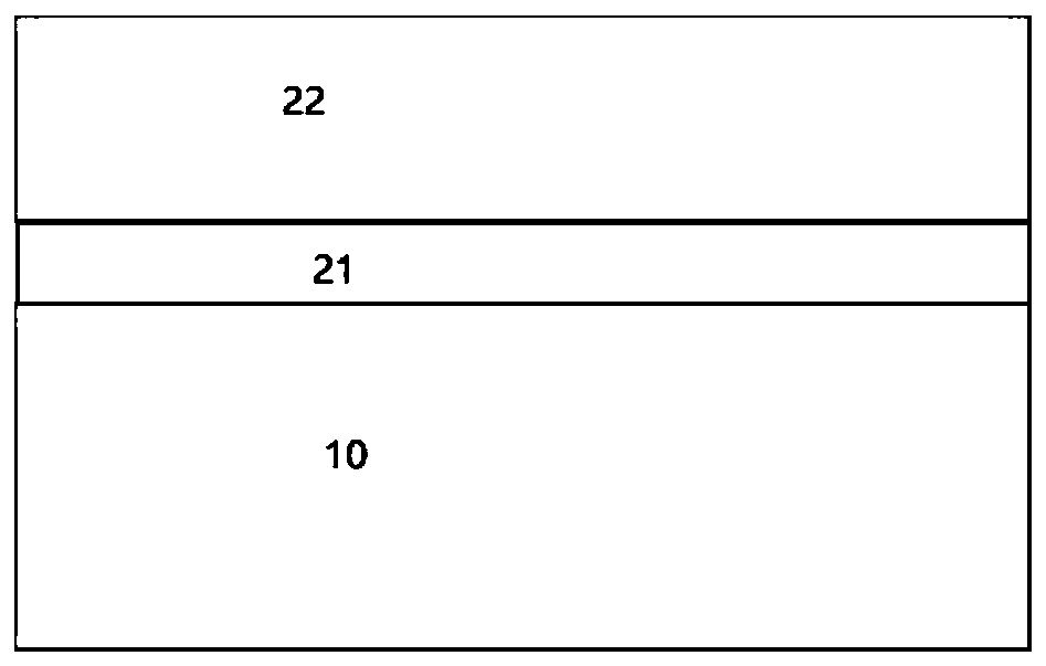
[0018] Take a single-sided polished N-type single wafer (resistivity 2Ω.cm, thickness 300um), pass POCL3 diffusion source at 1100°C for 30 minutes, oxidize, the oxide layer thickness is 0.5um, and take another N+ type single wafer (thickness 450um) chemical corrosion, RCA cleaning, Boil Concentrated Nitric Acid , spin dry, stick the two pieces together, bake in an oven at 200°C for 2 hours, then put them in a diffusion furnace at 1200°C for 6 hours, thin and polish until the thickness of the N-zone is 8um. The obtained diffusion zone is 13um, and the width of the transition zone 4um. Oxidize the polished surface at 1000°C to a thickness of 1um, photolithographically conduct the channel, etch the oxide layer, pass the POCL3 diffusion source at 1100°C for 30 minutes, and then put it in a diffusion furnace at 1200°C for 5 hours. The resulting diffusion area is 10um, which is the same as the diffusion sheet The N+ regions are connected. The other steps adopt the general planar ...


PUM


Abstract

The invention mainly aims to provide a novel vertical conductive structure coplanar electrode semiconductor discrete device and a preparation method thereof, and particularly relates to a semiconductor device prepared by using a diffusion type SOI silicon wafer and a preparation method thereof. According to the method, a shallow junction diffusion silicon wafer and a substrate silicon wafer playing a supporting role are adopted to replace an epitaxial wafer or a deep junction diffusion wafer with high cost through bonding of an insulating layer such as silicon dioxide, so that the cost is reduced; and the back electrode is led to the front surface and is coplanar with other front surface electrodes. In the manufacturing process, an active region silicon wafer is diffused firstly; then thesubstrate silicon wafer is bonded through an oxide layer to serve as a support; high-low concentration transition regions are reduced; a back high-concentration layer can be led to the front face through a diffusion high-concentration outer ring layer; and an electrode is formed. As shown in the figure structure, the silicon wafer is composed of a substrate slice 10, the diffusion silicon wafer and the insulating layer 20, and the diffusion silicon wafer comprises a high-concentration bottom area 30, a low-concentration area 40, a bottom electrode leading-out area high-concentration layer 50,other indicating areas such as an inversion layer 41, a coplanar electrode 70 / 80 and a dielectric layer 80. The structure can be widely used for leading vertically conducted semiconductor device electrodes to the same surface. A low-cost surface mounting device can be formed, and the application range is wide.

Description

technical field [0001] The invention belongs to the technical field of semiconductor devices and their preparation, and in particular relates to a semiconductor device which uses diffused SOI to bond silicon wafers and forms electrodes on the same plane and a preparation method thereof. Background technique [0002] Semiconductor discrete devices are divided into two methods: horizontal conduction and vertical conduction. Horizontal conduction devices can be formed with electrodes on the same surface, but the current conduction capability is poor, the power is low, and the chip area is large; vertical conduction devices are suitable for high-power applications. The current conduction ability is strong, but the electrodes are distributed on the front and back sides, which is not suitable for new packaging such as CSP. [0003] There are generally three methods for substrate growth used in vertical conduction devices: 1. Epitaxial growth. A low-concentration layer is grown by...

Claims


Application Information

Patent Timeline
IPC IPC(8): H01L21/762H01L27/12
CPCH01L21/76256H01L27/1203
Inventor 杨朔
Owner SHANGHAI ANWEI ELECTRONICS
Why Eureka
Try Eureka