Silicon carbide seed crystal and method for reducing penetration type dislocation density in silicon carbide single crystal

A silicon carbide single crystal and silicon carbide seed technology, which is applied in chemical instruments and methods, single crystal growth, single crystal growth and other directions, can solve the problems of stacking fault defects, reduced threading dislocation density, and complicated steps.

Inactive Publication Date: 2020-06-12
广州南砂晶圆半导体技术有限公司
View PDF0 Cites 1 Cited by
  • Summary
  • Abstract
  • Description
  • Claims
  • Application Information

AI Technical Summary

Problems solved by technology

For dislocations in SiC single crystals, the "Repeated A-Face (RAF)" method is currently used, that is, the alternate growth of the a-plane (11-20) and the m-plane (1-100) is repeated many times, and then the C-plane growth can obtain high-quality SiC single crystals with low dislocation density. However, this method requires multiple repeated growths, and the steps are complicated and other defects are easily introduced during repeated growths; there is also the possibility of setting SiC along the non-polar growth plane. Growth, compared with growth along the c-axis polar plane, shows completely different growth kinetics and defect generation mechanism, and the threading dislocation density is greatly reduced compared with growth along the c-axis, but this method will generate a large number of stacking fault defects

Method used


Image

  • Silicon carbide seed crystal and method for reducing penetration type dislocation density in silicon carbide single crystal
  • Silicon carbide seed crystal and method for reducing penetration type dislocation density in silicon carbide single crystal
  • Silicon carbide seed crystal and method for reducing penetration type dislocation density in silicon carbide single crystal

Examples


Embodiment Construction

[0034] Reference will now be made in detail to the exemplary embodiments, examples of which are illustrated in the accompanying drawings. When the following description refers to the accompanying drawings, the same numerals in different drawings refer to the same or similar elements unless otherwise indicated. The implementations described in the following exemplary examples do not represent all implementations consistent with the present invention. Rather, they are merely examples of apparatuses and methods consistent with aspects of the invention as recited in the appended claims.

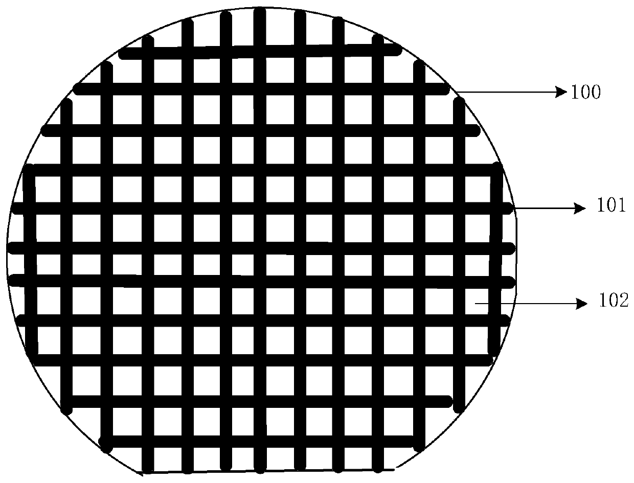
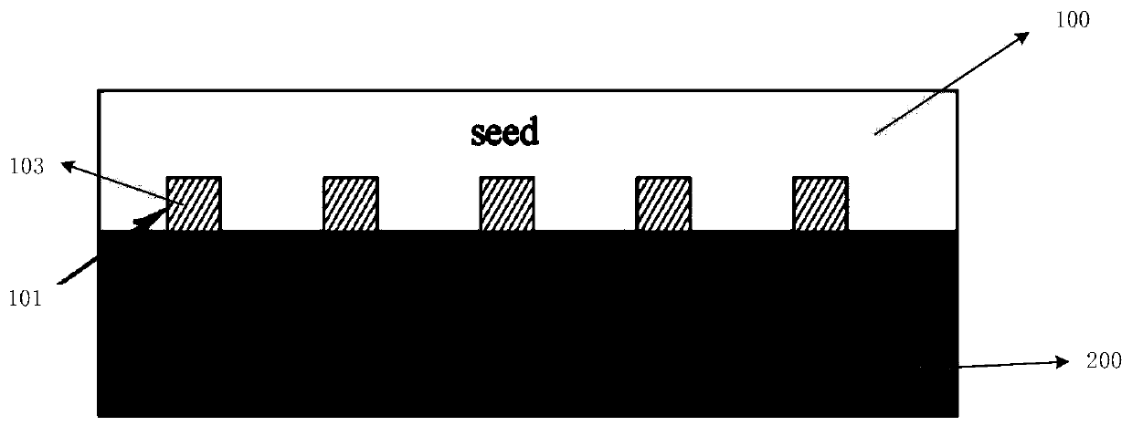
[0035] figure 1 A schematic diagram of the basic structure of a silicon carbide seed crystal provided in the embodiment of the present application. Such as figure 1 As shown, the SiC seed crystal 100 of this embodiment has a first surface and a second surface opposite to each other, wherein, in this embodiment, the surface used for bonding with the seed crystal holder is the second surface. I...


PUM

PropertyMeasurementUnit
widthaaaaaaaaaa
widthaaaaaaaaaa

Abstract

The invention provides a silicon carbide seed crystal and a method for reducing the penetration type dislocation density in a silicon carbide single crystal. A groove is formed in the back of the seedcrystal, the groove is filled with a material with the heat conductivity different from that of silicon carbide, or the back of the seed crystal is directly plated with a film with the heat conductivity different from that of the silicon carbide, so that two substances with the different heat conductivities exist on the back of the seed crystal, and uneven distribution of a temperature field on the surface of the seed crystal is caused when heat dissipation is uneven. Therefore, periodic distribution of the two substances with different thermal conductivities on the back of the seed crystal can be utilized, the distribution of a seed crystal surface temperature field in the SiC physical vapor transport growth process is modulated, preferential nucleation is forced to be carried out in a low-temperature area corresponding to a predefined pattern, selective preferential growth is carried out according to the predefined pattern, and then lateral growth is carried out, so that the purposeof reducing the penetration type dislocation density is achieved.

Description

technical field [0001] The present application relates to the technical field of silicon carbide single crystal growth, in particular to a silicon carbide seed crystal and a method for reducing threading dislocation density in a silicon carbide single crystal. Background technique [0002] As a representative of the third-generation wide bandgap semiconductor materials, silicon carbide materials have excellent physical and chemical properties such as large band gap, high carrier saturation migration velocity, high thermal conductivity, high critical breakdown electric field strength, and good chemical stability. . Based on these excellent characteristics, SiC materials are considered to be ideal materials for making high-frequency, high-power, high-temperature-resistant and radiation-resistant electronic devices. , nuclear reactor systems and military equipment and other fields have a wide range of applications. [0003] Growing large-diameter, high-quality SiC single crys...

Claims


Application Information

Patent Timeline
Patent Type & Authority Applications(China)
IPC IPC(8): C30B29/36C30B23/02
CPCC30B23/025C30B29/36
Inventor 杨祥龙徐现刚王垚浩于国建陈秀芳
Owner 广州南砂晶圆半导体技术有限公司
Why Eureka
Try Eureka