Semiconductor structure and forming method thereof

A semiconductor and layer-forming technology, applied in the fields of semiconductor devices, semiconductor/solid-state device manufacturing, and semiconductor/solid-state device components, etc., can solve problems that affect the normal operation of semiconductor devices, have a great impact on performance, and are difficult to process, and achieve guarantees Effects of electrical connection performance, improved process feasibility, improved yield and reliability

Active Publication Date: 2020-06-16
SEMICON MFG INT (SHANGHAI) CORP +1
View PDF4 Cites 0 Cited by
  • Summary
  • Abstract
  • Description
  • Claims
  • Application Information

AI Technical Summary

Problems solved by technology

With the advancement of technology nodes, the size of the interconnection structure becomes smaller and smaller; correspondingly, the process difficulty of forming the interconnection structure is also increasing, and the formation quality of the interconnection structure has a great impact on the back end offline , BEOL) The performance of the circuit is greatly affected, and in severe cases, it will affect the normal operation of semiconductor devices

Method used


Image

  • Semiconductor structure and forming method thereof
  • Semiconductor structure and forming method thereof
  • Semiconductor structure and forming method thereof

Examples


Embodiment Construction

[0013] Currently, the yield and reliability of semiconductor structures need to be improved. Combining with a method of forming a semiconductor structure, the reasons for its yield and reliability decline are analyzed.

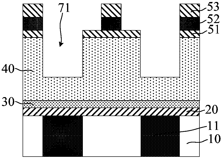
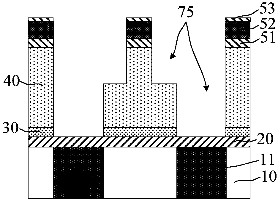
[0014] refer to Figure 1 to Figure 6 , shows a structural schematic diagram corresponding to each step in a method for forming a semiconductor structure.

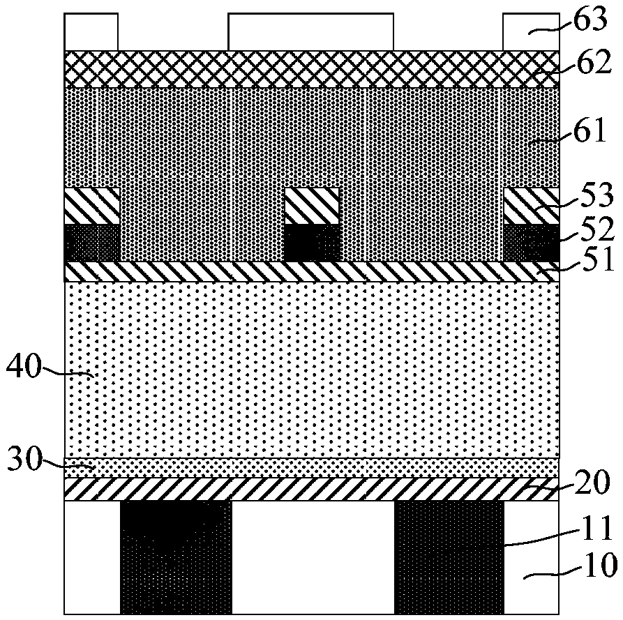
[0015] refer to figure 1 , providing a substrate (not shown), on which a front dielectric layer 10 and a front interconnect structure 11 located in the front dielectric layer 10 are formed, the front interconnect structure 11 and the front dielectric The top of the layer 10 is flush; an etch stop layer 20 is formed on the front dielectric layer 10, and the etch stop layer 20 covers the front interconnect structure 11; a transition layer is formed on the etch stop layer 20 30; forming an interlayer dielectric layer 40 on the transition layer 30; forming an etching buffer layer 51 on the interlayer dielec...


PUM


Abstract

The invention relates to a semiconductor structure and a forming method thereof. The forming method comprises the following steps that: a substrate is provided, a front dielectric layer and a front interconnection structure located in the front dielectric layer are formed on the substrate, the front dielectric layer exposes the top of the front interconnection structure; a protective layer is formed on the front interconnection structure; an interlayer dielectric layer is formed on the front dielectric layer, wherein the interlayer dielectric layer covers the protective layer; a graphical hardmask layer is formed on the interlayer dielectric layer; the interlayer dielectric layer is patterned with the hard mask layer adopted as a mask, so that an interconnection opening can be formed, andpenetrates through the interlayer dielectric layer above the front interconnection structure; the hard mask layer is removed; after the hard mask layer is removed, the interconnection opening is filled, so that an interconnection structure can be formed. With the semiconductor structure and the forming method thereof of the invention adopted, the feasibility of removing the hard mask layer beforethe interconnection opening is filled is improved. Compared with a scheme of filling the interconnection opening under the condition of reserving the hard mask layer, the method of the invention candecrease the depth-to-width ratio of a space filled with an interconnection structure material is reduced, so that the filling capability of the interconnection structure in the interconnection opening is improved.

Description

technical field [0001] Embodiments of the present invention relate to the field of semiconductor manufacturing, and in particular, to a semiconductor structure and a method for forming the same. Background technique [0002] With the continuous development of integrated circuit manufacturing technology, people's requirements for the integration and performance of integrated circuits are becoming higher and higher. In order to improve integration and reduce costs, the critical dimensions of components are getting smaller and the circuit density inside integrated circuits is increasing. This development makes the surface of the wafer unable to provide enough area to make the required interconnection lines. [0003] In order to meet the requirements of the interconnection line after the critical dimension is reduced, at present, the conduction between different metal layers or the metal layer and the substrate is realized through the interconnection structure. With the advance...

Claims


Application Information

Patent Timeline
IPC IPC(8): H01L21/768H01L23/528H01L23/532
CPCH01L23/5283H01L21/76808H01L21/76813H01L23/5329H01L23/53257
Inventor 袁可方罗杰黄敬勇
Owner SEMICON MFG INT (SHANGHAI) CORP
Why Eureka
Try Eureka