Eureka AIR delivers breakthrough ideas for toughest innovation challenges, trusted by R&D personnel around the world.

Electronic component and electronic device

A technology of electronic components and devices, which is applied in the direction of electrical components, electrical connection printed components, printed circuits connected with non-printed electrical components, etc., can solve the problems of lower yield rate, increase of defective parts placement, and tin connection. Achieve the effect of reducing the arrangement density, improving the yield rate, and preventing tinning

Active Publication Date: 2020-06-19
GOERTEK OPTICAL TECH CO LTD
View PDF7 Cites 0 Cited by
  • Summary
  • Abstract
  • Description
  • Claims
  • Application Information

AI Technical Summary

Problems solved by technology

[0002] At present, the electronic product industry, especially consumer electronics, has higher and higher requirements for product miniaturization, thinning and aesthetic appearance, which increases the difficulty of packaging electronic devices, especially parts that are closely related to the appearance of the whole machine. On the one hand, it must be small , the overall package size is reduced, and the number of parts pins remains unchanged, so that the pin size and spacing are reduced, which increases the difficulty of the back-end circuit board process and part placement process, resulting in an increase in parts placement defects
In electronic equipment, in order to reduce the size (especially the height) of electronic components, the industry has canceled the shell package, and adopted some improved package designs to reduce the overall size, but at the same time caused electronic components to be used for electrical connection with external circuits The increase in the arrangement density of the connection points leads to the easy tin connection of electronic components during the subsequent manufacturing process, which greatly reduces the yield of production

Method used


Image

  • Electronic component and electronic device
  • Electronic component and electronic device
  • Electronic component and electronic device

Examples


Embodiment Construction

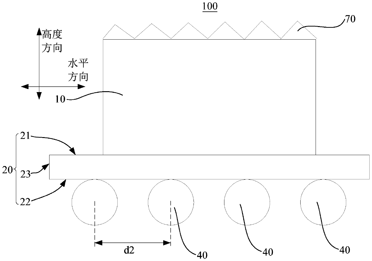
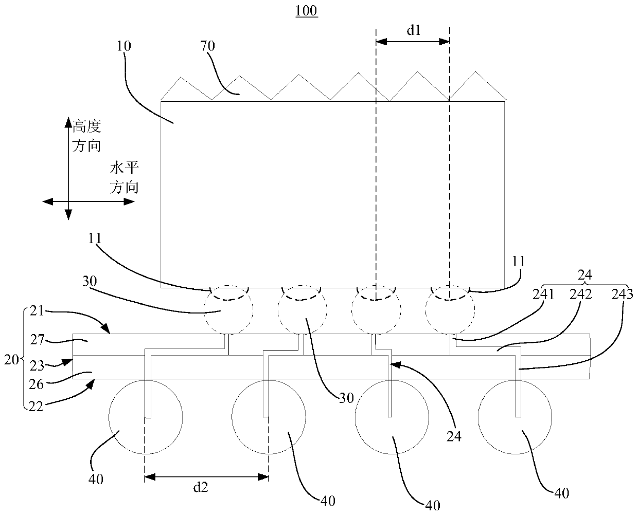
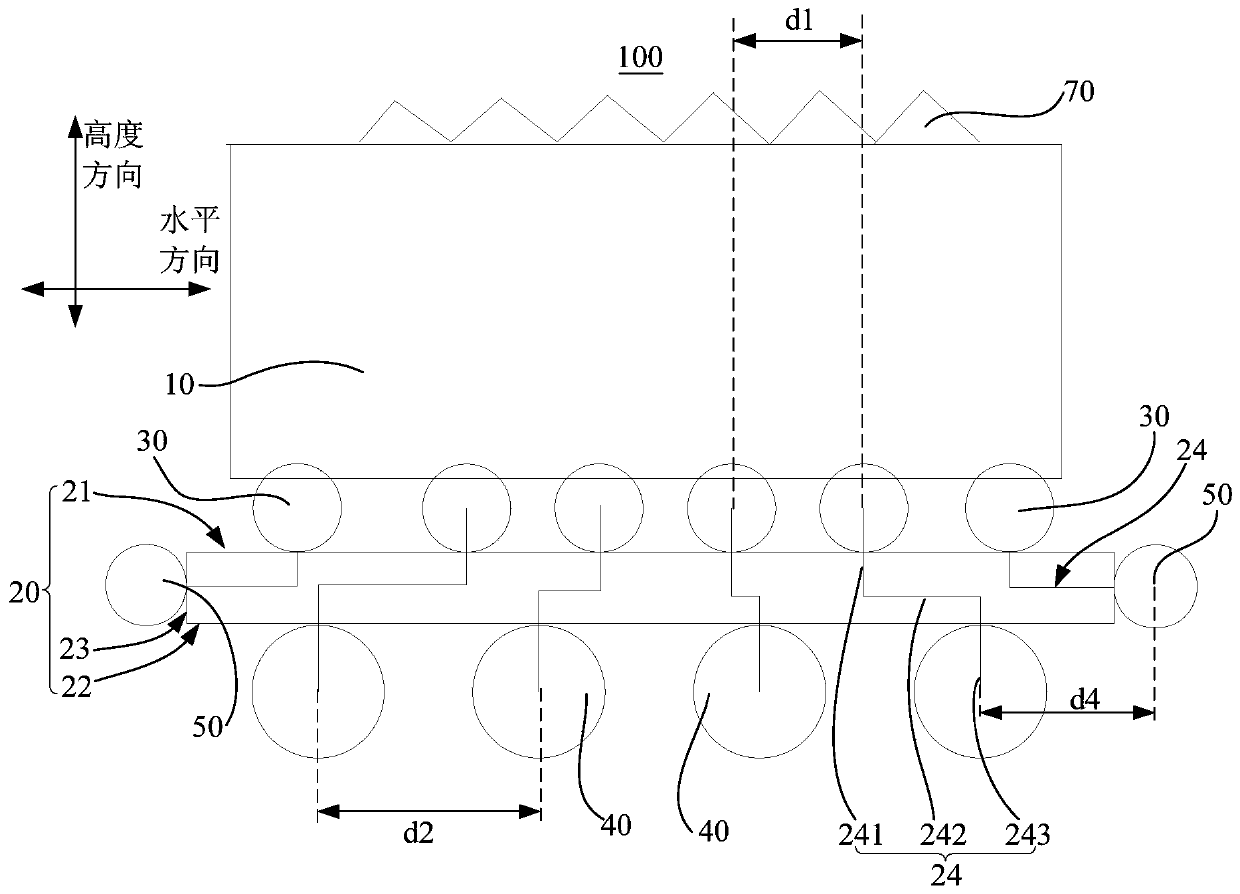
[0037] The following will clearly and completely describe the technical solutions in the embodiments of the present invention with reference to the accompanying drawings in the embodiments of the present invention. Obviously, the described embodiments are only part of the embodiments of the present invention, not all of them. Based on the embodiments of the present invention, all other embodiments obtained by persons of ordinary skill in the art without creative efforts fall within the protection scope of the present invention.

[0038] It should be noted that all directional indications (such as up, down, left, right, front, back...) in the embodiments of the present invention are only used to explain the relationship between the components in a certain posture (as shown in the accompanying drawings). Relative positional relationship, movement conditions, etc., if the specific posture changes, the directional indication also changes accordingly.

[0039] In addition, the desc...


PUM


Abstract

The invention discloses an electronic component and an electronic device, and the electronic component comprises a device body, one surface of the device body being uniformly provided with a pluralityof connection points, each connection point being communicated with an internal circuit of the device body, and the distance between two adjacent connection points being d1; and a connecting plate, the connecting plate comprising a first surface and a second surface which are oppositely arranged. A plurality of second solder balls are arranged on the second surface. The surface, provided with theconnecting points, of the device body is arranged on the first surface in an attached mode, each second solder ball is electrically connected with one connecting point, and the relation between the distance d2 between every two adjacent second solder balls and the distance d1 between every two adjacent connecting points is d2 > d1. According to the technical scheme, the arrangement density of thejoint, used for being electrically connected with an external circuit, of the electronic component is reduced, tin connection of the electronic component in the subsequent manufacturing process is prevented, and the production yield is increased.

Description

technical field [0001] The invention relates to the technical field of semiconductors, in particular to electronic components and electronic equipment. Background technique [0002] At present, the electronic product industry, especially consumer electronics, has higher and higher requirements for product miniaturization, thinning and aesthetic appearance, which increases the difficulty of packaging electronic devices, especially parts that are closely related to the appearance of the whole machine. On the one hand, it must be small , the overall package size is reduced, the number of parts pins remains unchanged, the pin size and spacing are reduced, and it is more difficult for the back-end circuit board process and part placement process, resulting in an increase in part placement defects. In electronic equipment, in order to reduce the size (especially the height) of electronic components, the industry has canceled the shell package, and adopted some improved package des...

Claims


Application Information

Patent Timeline
Patent Type & Authority Applications(China)
IPC IPC(8): H05K1/11H05K1/18
CPCH05K1/181H05K1/111H05K2201/09372
Inventor 李敬丁卫涛
Owner GOERTEK OPTICAL TECH CO LTD
Why Eureka
Eureka Blog
Learn More