Packaging component and preparation method thereof

A technology for encapsulating components and encapsulating colloids, which is applied in the manufacture of semiconductor/solid-state devices, electrical components, and electrical solid-state devices. Effect

Active Publication Date: 2020-06-26
深圳市之诺微电子有限公司
View PDF3 Cites 2 Cited by
  • Summary
  • Abstract
  • Description
  • Claims
  • Application Information

AI Technical Summary

Problems solved by technology

However, the heat dissipation capability of conventional semiconductor packaging components is limited, therefore, it is necessary to provide a semiconductor packaging component with better heat dissipation performance in this technical field

Method used


Image

  • Packaging component and preparation method thereof
  • Packaging component and preparation method thereof

Examples


Embodiment Construction

[0026] Embodiments of the present invention are described below through specific examples, and those skilled in the art can easily understand other advantages and effects of the present invention from the content disclosed in this specification. The present invention can also be implemented or applied through other different specific implementation modes, and various modifications or changes can be made to the details in this specification based on different viewpoints and applications without departing from the spirit of the present invention. Based on the embodiments of the present invention, all other embodiments obtained by persons of ordinary skill in the art without making creative efforts belong to the protection scope of the present invention.

[0027] A method for preparing a packaging component proposed by the present invention comprises the following steps:

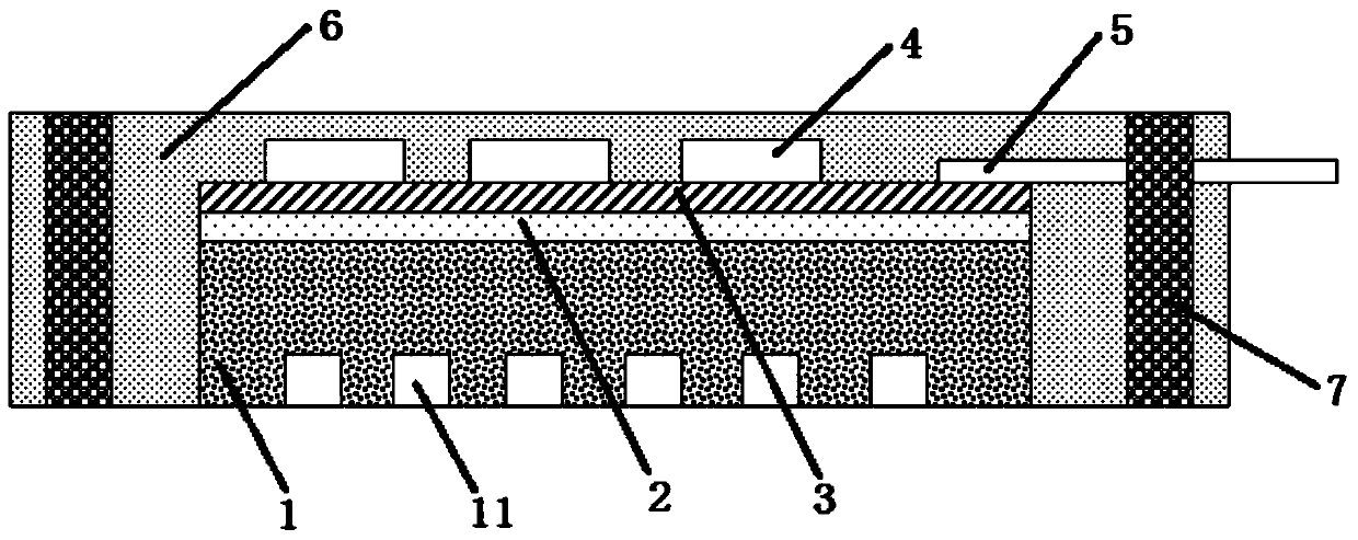
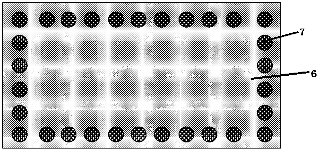
[0028] 1) Provide a heat dissipation substrate, the heat dissipation substrate has a first surface and a sec...


PUM

PropertyMeasurementUnit
diameteraaaaaaaaaa
thicknessaaaaaaaaaa
thicknessaaaaaaaaaa

Abstract

The invention relates to a packaging component and a preparation method thereof. The method comprises the following steps of providing a heat dissipation substrate, and etching the second surface of the heat dissipation substrate to form a plurality of concave holes; forming an insulating layer and a circuit wiring layer on the first surface of the heat dissipation substrate; mounting a pluralityof semiconductor elements and a plurality of conductive pins on the circuit wiring layer; forming a packaging colloid; forming a plurality of through holes at the periphery of the packaging colloid atintervals, wherein the through holes penetrate through the packaging colloid; providing a plurality of metal conductive columns, and forming a plurality of through holes penetrating through the metalconductive columns on the side surfaces of the metal conductive columns, embedding the plurality of metal conductive columns into the corresponding through holes respectively, and performing a thermal compression bonding process on the packaging colloid to enable part of the packaging colloid to be embedded into the through holes of the metal conductive columns.

Description

technical field [0001] The invention relates to the technical field of semiconductor packaging, in particular to a packaging component and a preparation method thereof. Background technique [0002] In a conventional manufacturing process of a semiconductor package component, a semiconductor element is electrically connected to a package substrate through a solder material. The semiconductor element is placed on the packaging substrate and aligned to the placement site so that the solder balls are aligned with the pads on the substrate. Then, a reflow soldering process is used to fixedly connect the semiconductor element and the package substrate. For semiconductor packaging components, there are two major challenges in electrical performance and heat dissipation control. In particular, in terms of heat dissipation control, semiconductor package members are required to effectively dissipate heat generated by semiconductor elements. Heat sinks are usually attached to subst...

Claims


Application Information

Patent Timeline
Patent Type & Authority Applications(China)
IPC IPC(8): H01L23/367H01L23/373H01L21/56H01L23/31
CPCH01L21/56H01L23/3114H01L23/3677H01L23/3736
Inventor 张正
Owner 深圳市之诺微电子有限公司
Why Eureka
Try Eureka