Ultraviolet LED epitaxial structure and preparation method thereof

An epitaxial structure, ultraviolet technology, applied in semiconductor devices, electrical components, circuits, etc., can solve the problems of large growth stress of epitaxial layer, easy capture of electrons and holes, white light, etc., to improve crystal quality and optical output power, improve The effect of deep ultraviolet light whitening and reducing dislocation density

Active Publication Date: 2020-06-26
江西力特康光学有限公司
View PDF13 Cites 8 Cited by
  • Summary
  • Abstract
  • Description
  • Claims
  • Application Information

AI Technical Summary

Problems solved by technology

The AlGaN material is located on the side of the AlN buffer layer away from the substrate, and the most commonly used substrate is sapphire (Al 2 o 3 ), the large lattice mismatch and thermal mismatch between the AlN buffer layer and the sapphire substrate will introduce a large number of dislocations, and will also lead to a large growth stress of the epitaxial layer, which is easy to crack during the cooling process
Moreover, after the AlN buffer layer is grown, AlGaN materials such as non-doped AlGaN layer or N-type AlGaN ohmic contact layer are grown immediately. Due to the difference in lattice constant, the dislocation density will further increase, and a large number of threading dislocations will proliferate upwards. , so that defects appear in AlGaN and it is easy to trap electrons and holes, resulting in the phenomenon of white light
In addition, the high stress in the growth process of AlGaN will also lead to cracks on the surface, especially the edges, which will reduce the usable area and reduce the output rate.

Method used


Image

  • Ultraviolet LED epitaxial structure and preparation method thereof
  • Ultraviolet LED epitaxial structure and preparation method thereof
  • Ultraviolet LED epitaxial structure and preparation method thereof

Examples


Embodiment Construction

[0047] Various exemplary embodiments of the present invention will now be described in detail with reference to the accompanying drawings. It should be noted that the relative arrangements of components and steps, numerical expressions and numerical values ​​set forth in these embodiments do not limit the scope of the present invention unless specifically stated otherwise.

[0048] The following description of at least one exemplary embodiment is merely illustrative in nature and in no way taken as limiting the invention, its application or uses.

[0049] Techniques, methods and devices known to those of ordinary skill in the relevant art may not be discussed in detail, but where appropriate, such techniques, methods and devices should be considered part of the description.

[0050] In all examples shown and discussed herein, any specific values ​​should be construed as exemplary only, and not as limitations. Therefore, other instances of the exemplary embodiment may have dif...


PUM


Abstract

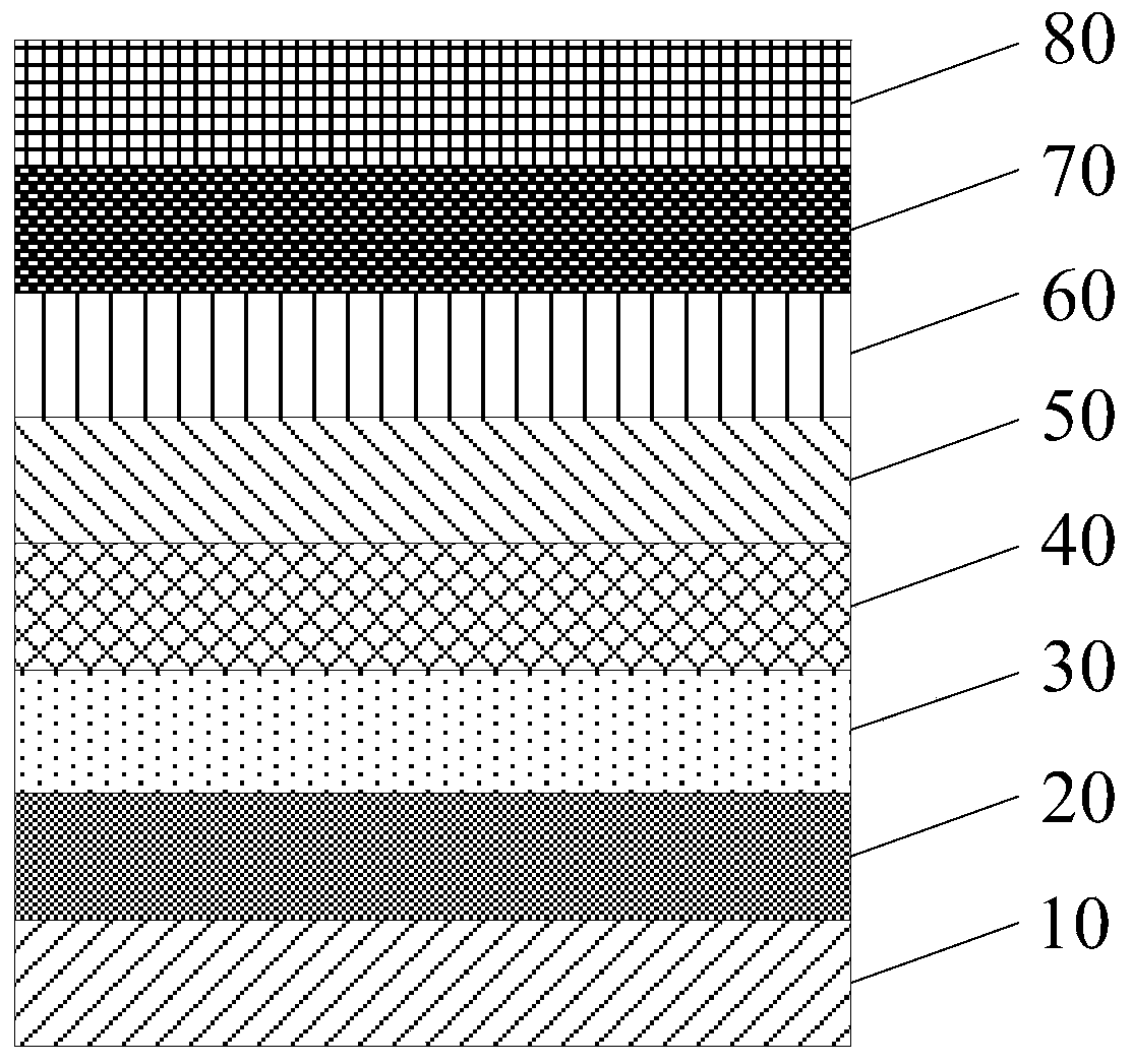
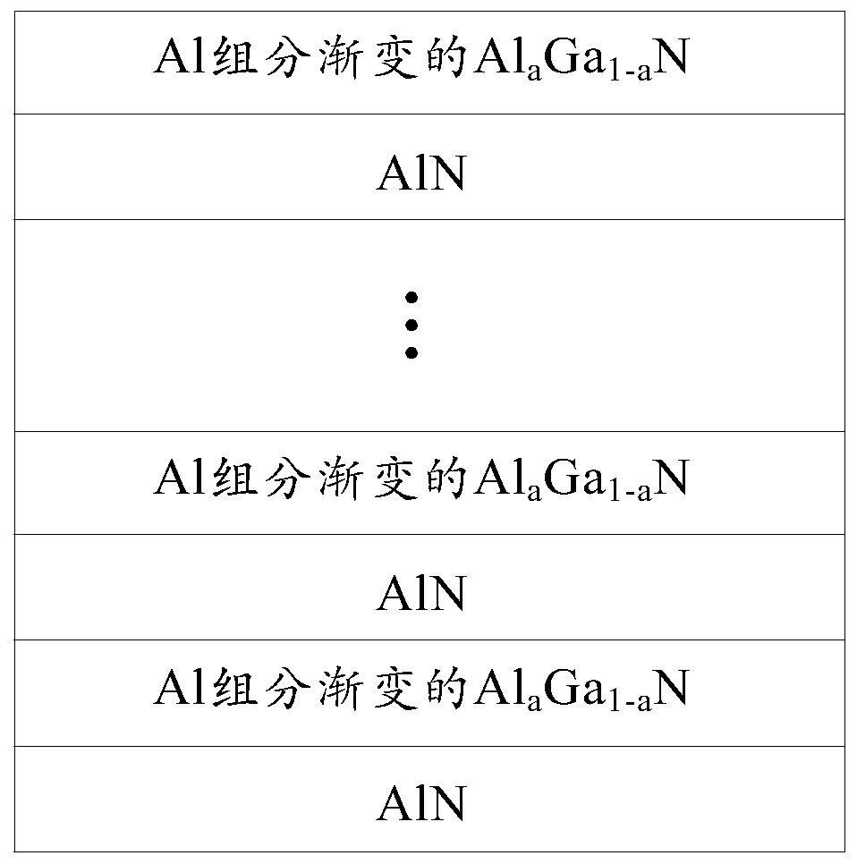
The invention provides an ultraviolet LED epitaxial structure and a preparation method thereof, and relates to the light-emitting diode technical field. The epitaxial structure comprises a substrate,a first AlN layer, a second AlN layer, an AlN/AlGaN superlattice stress release layer, an N-type AlcGa1-cN ohmic contact layer and an AlxGa1-xN/AlyGa1-yN multi-quantum well active region, wherein theAlN/AlGaN superlattice stress release layer at least comprises a first superlattice and a second superlattice, the AlN/AlGaN superlattice stress release layer can effectively relieve the strain between the second AlN layer and the N-type AlcGa1-cN ohmic contact layer, and the gradually changed Al component in the superlattice can reduce the dislocation density and gradually release the stress caused by lattice mismatch, so that the crack-free and high-quality ultraviolet LED epitaxial structure is obtained, the output power of a deep ultraviolet LED is improved, and the phenomenon of deep ultraviolet whitening is improved.

Description

technical field [0001] The present invention relates to the technical field of light-emitting diodes, and more particularly, to an epitaxial structure of an ultraviolet LED (Light-Emitting Diode, light-emitting diode) and a preparation method thereof. Background technique [0002] In recent years, with the characteristics of safety, small size, environmental protection, high efficiency, and low energy consumption, ultraviolet LED light sources have gradually replaced traditional mercury lamp light sources, and their market share has increased year by year with great potential. The application of ultraviolet LEDs in the field of sterilization and disinfection has received unprecedented attention and attention. [0003] Usually, in the process of manufacturing an ultraviolet LED, an AlN buffer layer and an AlGaN material are sequentially grown on the surface of the substrate. The AlGaN material is located on the side of the AlN buffer layer away from the substrate, and the mo...

Claims


Application Information

Patent Timeline
Patent Type & Authority Applications(China)
IPC IPC(8): H01L33/04H01L33/06H01L33/12H01L33/14H01L33/32H01L33/00
CPCH01L33/0075H01L33/04H01L33/06H01L33/12H01L33/145H01L33/32
Inventor 刘锐森蓝文新刘召忠林辉杨小利
Owner 江西力特康光学有限公司
Why Eureka
Try Eureka