

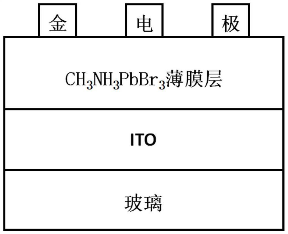
A write-once-read-many memory based on hybrid perovskite and its preparation method
A multi-read, perovskite technology, which is applied in semiconductor/solid-state device manufacturing, semiconductor devices, electric solid-state devices, etc. Improvement and other issues, to achieve the effect of simple preparation method, simplified process flow and low misreading rate
- Summary
- Abstract
- Description
- Claims
- Application Information
AI Technical Summary
Problems solved by technology
Method used
Image

Examples
Embodiment 1
[0044] (1) Cleaning ITO
[0045] The ITO conductive glass is first accepted for 30 minutes in deionized water, acetone, alcohol, and then irradiate the ITO surface with ultraviolet light in the UV cleaning device for 20 minutes;
[0046] (2) Configuring a calcium titanium ore precursor solution
[0047] 0.229 g of bromide and 0.070 g of bromide were weighed in 1: 1, mixed in a 1 ml acetate solution, and then stirred at 60 ° C for 2 hours, prepared calcium titanium concentrations of 300 mg / mL. Mine precursor solution;
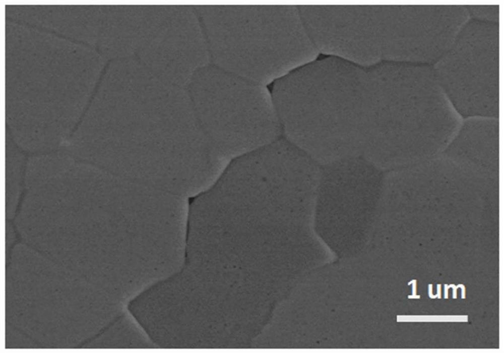
[0048] (3) Preparation of perovskite film
[0049] In the air environment, the ITO substrate in step (1) was heated to 90 ° C, and the propanmetric precursor solution in step (2) was taken in the surface of the propanoform, and the spin coater rotational speed was set to 4000 rpm. Time is 20s, then annealed at 100 ° C for 5 min, resulting in a curing calcium titanium ore active layer having a thickness of 300 nm, and its surface topography is figure 2 Indicated; ...
Embodiment 2
[0055] (1) Cleaning ITO
[0056] The ITO conductive glass is first in terms of deionized water, acetone, alcohol, and then irradiate the ITO surface for 15 minutes with ultraviolet light in the UV cleaning instrument;
[0057] (2) Configuring a calcium titanium ore precursor solution
[0058] 0.229 g of bromide and 0.070 g of bromide were weighed in 1: 1, mixed in a 1 ml acetate solution, and then stirred at 60 ° C for 2 hours, prepared calcium titanium concentrations of 300 mg / mL. Mine precursor solution;
[0059] (3) Preparation of perovskite film
[0060] In the air environment, the ITO substrate in step (1) was heated to 100 ° C, and the propanmetric precursor solution in step (2) was used to spin coating in the surface of the perovskite precursor solution in step (2), and the spin coater speed was set to 4000 rpm. Time is 20s, then annealed at 100 ° C for 5 min, resulting in a curing calcium-titanium ore active layer having a thickness of 300 nm;
[0061] (4) Preparation to...
Embodiment 3
[0066] (1) Cleaning ITO
[0067] The ITO conductive glass is first accepted for 30 minutes in deionized water, acetone, alcohol, and then irradiate the ITO surface with ultraviolet light in the UV cleaning device for 20 minutes;
[0068] (2) Configuring a calcium titanium ore precursor solution
[0069] 0.229 g of bromide and 0.070 g of bromide were weighed in 1: 1, mixed in a 1 ml acetate solution, and then stirred at 60 ° C for 2 hours, prepared calcium titanium concentrations of 300 mg / mL. Mine precursor solution;
[0070] (3) Preparation of perovskite film
[0071] In the air environment, the ITO substrate in step (1) is heated to 90 ° C, and the propanoferous precursor solution in step (2) is used to spin coating in the ITO surface using the pipette amount of the pipette, and the spin coater speed is set to 3000 rpm. The time is 20s, then annealed at 90 ° C for 5 min, resulting in a curing calcium-titanium ore active layer having a thickness of 350 nm;
[0072] (4) Preparat...
PUM
| Property | Measurement | Unit |
|---|---|---|
| thickness | aaaaa | aaaaa |
| width | aaaaa | aaaaa |
| thickness | aaaaa | aaaaa |
Abstract
Description
Claims
Application Information