
Heterogeneously integrated CWDM4 light emitting chip

A transmitter chip and heterogeneous technology, applied in the field of integrated optical transceiver chips, can solve the problems of application limitations, large optical loss, and large power consumption, and achieve low transmission optical loss, small transmission loss, and small mode field mismatch Effect

Pending Publication Date: 2020-06-26
HENGTONG ROCKLEY TECHNOLOGY CO LTD
View PDF0 Cites 4 Cited by
  • Summary
  • Abstract
  • Description
  • Claims
  • Application Information

AI Technical Summary

Problems solved by technology

However, the integrated optical emission chip based on pure silicon waveguide also has a disadvantage that the optical loss is too large, resulting in too weak emitted optical signal or excessive power consumption, which is greatly limited in application.
Compared with optical devices based on silicon waveguides and their integrated chips, based on PLC waveguides (the waveguide material is SiO 2 ) optical devices and integrated chips have very low optical loss, and match the mode field of single-mode fiber, but its disadvantage is that it cannot realize high-speed electro-optic modulation

Method used


Image

  • Heterogeneously integrated CWDM4 light emitting chip
  • Heterogeneously integrated CWDM4 light emitting chip
  • Heterogeneously integrated CWDM4 light emitting chip

Examples


Embodiment

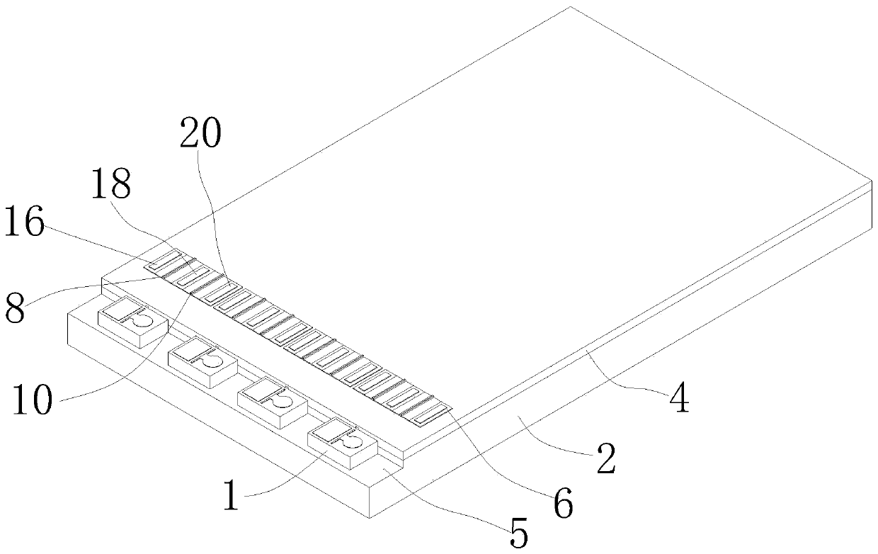
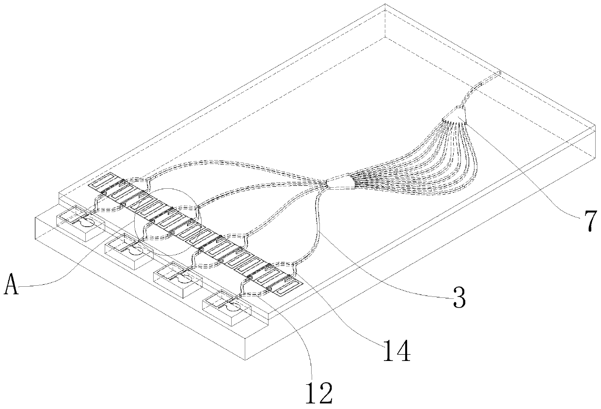
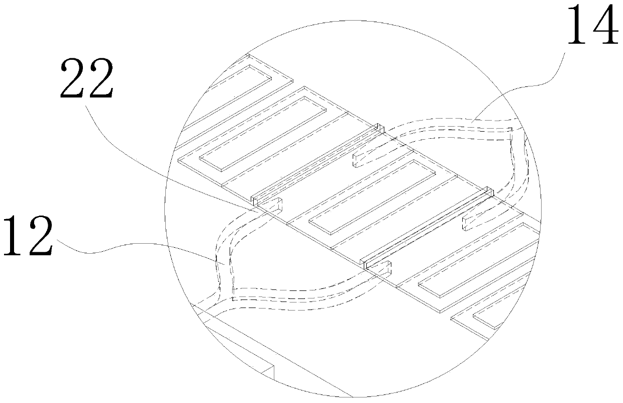
[0031] This embodiment discloses a light emitting chip suitable for CWDM4 optical module, refer to Figure 1~4 As shown, the light-emitting chip has a substrate 2, a SiO 2 Layer 4 and Si layer 6; the light emitting chip is integrated with four MZ electro-optic modulators, four lasers 1 with different wavelengths and a wavelength division multiplexer 7, and the wavelength division multiplexer 7 is arranged on SiO 2 In layer 4, a PLC waveguide wavelength division multiplexer is preferably used; here, the PLC waveguide wavelength division multiplexer 7 is a wavelength division multiplexer that uses a PLC waveguide to transmit optical signals.

[0032] The above four lasers 1 are sequentially bonded on the substrate 2 . Among them, the step groove 5 is processed on the above-mentioned substrate 2 through an etching process, and four lasers 1 with different wavelengths are arranged in a "one" shape, and are integrated on the step groove 5 through a bonding process. The depth of th...


PUM


Abstract

The invention discloses a heterogeneous integrated CWDM4 light emitting chip which integrates four MZ electro-optical modulators, four lasers and a wavelength division multiplexer, the four lasers arebonded on a substrate, a SiO2 layer is arranged on the substrate, and a Si layer is arranged on the SiO2 layer; each MZ electro-optical modulator comprises a PLC waveguide combiner, a PLC waveguide shunt and a pair of silicon waveguide phase shift arms; PLC waveguide combiners and demultiplexers of the four MZ electro-optical modulators are all arranged in the SiO2 layer, and silicon waveguide phase shift arms of the four MZ electro-optical modulators are all arranged on the Si layer. The wavelength division multiplexer is arranged in the SiO2 layer; optical signals output by the four lasersare coupled into the PLC waveguide splitters of the four MZ electro-optical modulators through end faces respectively, and the output ends of the PLC waveguide combiners of the four MZ electro-opticalmodulators are connected with the wavelength division multiplexer through PLC waveguides respectively. The heterogeneous integrated CWDM4 light emitting chip has the technical advantages of high modulation rate and low loss, and can directly realize low-loss end surface coupling with a single-mode optical fiber at a light emitting end.

Description

technical field [0001] The invention relates to the technical field of integrated optical transceiver chips, in particular to a light emitting chip, in particular to a heterogeneously integrated CWDM4 light emitting chip. Background technique [0002] Silicon-based integrated optical transceiver chips support 100G / 400G and even 800G high-speed transmission, and also support COB packaging technology, which has great advantages in terms of integration and cost. The 100G / 400G CWDM4 silicon-based integrated optical transmitter (TX) chip integrates 4 silicon-based electro-optical modulators, 1 silicon-based wavelength division multiplexer and 4 lasers with different wavelengths, and the wavelength division multiplexer can realize 4 Single-fiber transmission of optical signals with different wavelengths. At present, the integrated optical emission chip based on pure silicon waveguide has great advantages over other technical solutions in terms of single-channel modulation rate, n...

Claims


Application Information

Patent Timeline
Patent Type & Authority Applications(China)
IPC IPC(8): H04B10/50H04B10/516
CPCH04B10/503H04B10/516
Inventor 王皓朱宇陈奔施伟明吴邦嘉沈笑寒张拥建洪小刚邢园园田桂霞
Owner HENGTONG ROCKLEY TECHNOLOGY CO LTD
Learn More