Controllable processing method and device for nanopore array based on optical control

A nano-hole array, optical manipulation technology, applied in the process of producing decorative surface effects, micro-structure devices, manufacturing micro-structure devices, etc., can solve the application space limitation, dependence, uniformity and consistency requirements of gold nano-particle arrays Very high and other problems, to achieve the effect of broad application prospects

Active Publication Date: 2020-06-30
GUANGDONG UNIV OF TECH
View PDF12 Cites 4 Cited by
  • Summary
  • Abstract
  • Description
  • Claims
  • Application Information

AI Technical Summary

Problems solved by technology

Chinese patent CN102732885A proposes a magnetic field-assisted micro-nano processing technology, which transfers the required pattern through the photolithography process, then coats the metal for catalysis, adds an etching solution, and places it in a magnetic field environment with adjustable magnetic field strength and direction. Etching, due to the

Method used


Image

  • Controllable processing method and device for nanopore array based on optical control
  • Controllable processing method and device for nanopore array based on optical control
  • Controllable processing method and device for nanopore array based on optical control

Examples


Embodiment Construction

[0029] The technical solutions of the present invention will be further described below in conjunction with the accompanying drawings and through specific implementation methods.

[0030] The controllable processing method of the nanohole array based on optical manipulation in this embodiment includes the following steps:

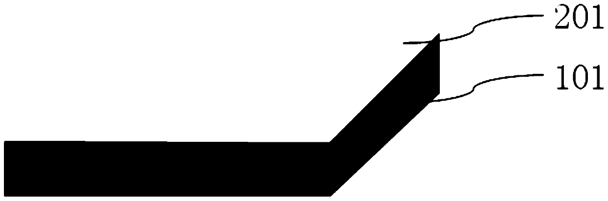
[0031] Step (1), such as figure 1 As shown, spin-coat one layer of cetyltrimethylammonium chloride layer 201 on the upper surface of the cleaned silicon wafer 101;

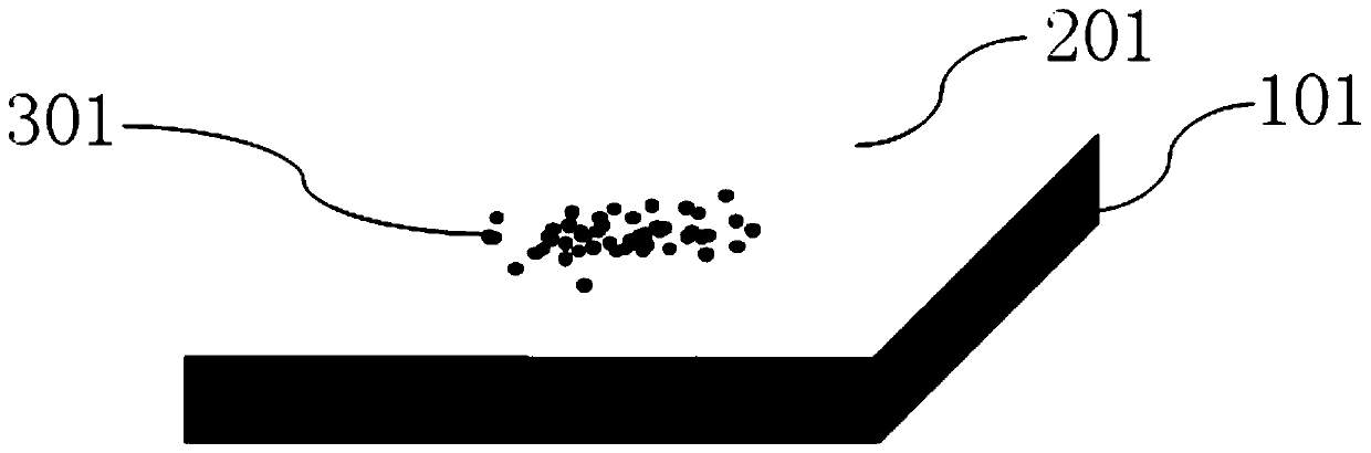
[0032] Step (2), such as figure 2 As shown, a layer of gold nanoparticles 301 is self-assembled on the upper surface of the silicon wafer 101 after step (1), and a disordered gold nanoparticle array 404 is formed on the silicon wafer 101;

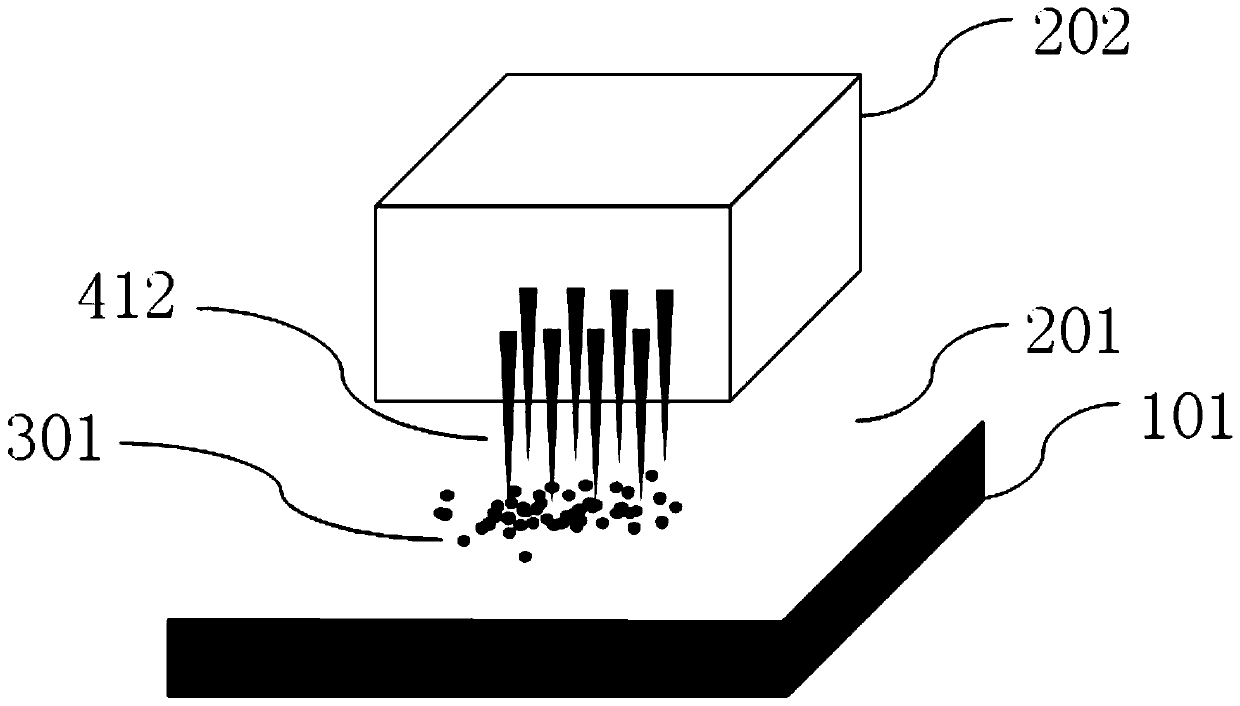
[0033] Step (3), such as image 3 As shown, the array laser beam 412 is dispersed by the multi-beam galvanometer 202, and the array laser beam 412 disperses the gold nanoparticles 301 in the disordered gold nanoparticle array 404 of step (2), as Figure...


PUM

PropertyMeasurementUnit
Wavelengthaaaaaaaaaa

Abstract

The invention discloses a controllable processing method and device of a nanopore array based on optical control. The method comprises the following steps: (1) spin-coating a hexadecyl trimethyl ammonium chloride layer on the upper surface of a cleaned silicon wafer, (2) self-assembling a layer of gold nanoparticles on the upper surface of the silicon wafer subjected to the step (1), (3) dispersing an array laser beam through a multi-beam galvanometer, and (4) performing optical manipulation on each gold nanoparticle through a single laser beam so as to enable each gold nanoparticle to move toa corresponding target position. The limitation of Van der Waals' force during self-assembly of the gold nanoparticles is overcome, according to the method, the customized gold nanoparticle array isaccurately processed at the designated position, and the high-quality silicon nanopore array is efficiently processed through metal-assisted chemical etching, so that the defects of large required process experiment workload, high hole site adjustment difficulty and the like of the conventional nanopore array etching technology are overcome, and the method has a wide application prospect.

Description

technical field [0001] The invention relates to the field of processing solid-state nanohole arrays, in particular to a controllable processing method and device for nanohole arrays based on optical manipulation. Background technique [0002] With the development of nanoscience and technology, the application of nanopore sensors in the fields of gene sequencing and energy conversion has made great progress. Solid-state nanopores have attracted the interest of many researchers due to their stable performance, controllable geometry and excellent robustness. At present, the field of single nanopore processing is relatively mature, but there are still many challenges for nanopore arrays that meet commercial applications such as gene sequencing, such as high processing costs, low efficiency, and poor controllability. Therefore, it is urgent to propose new methods to accurately process high-quality solid-state nanohole arrays, so as to accelerate the industrialization of solid-st...

Claims


Application Information

Patent Timeline
IPC IPC(8): B81C1/00
CPCB81C1/00031B81C1/00523B81C1/00539
Inventor 陈云陈燕辉丁树权施达创陈新高健刘强
Owner GUANGDONG UNIV OF TECH
Why Eureka
Try Eureka