Transmission electron microscope in-situ electrothermal coupling chip and preparation method thereof

A technology of electrothermal coupling and transmission electron microscopy, applied in circuits, discharge tubes, electrical components, etc., can solve problems such as electrical conductivity improvement

Active Publication Date: 2020-06-30
XIAMEN CHIP NOVA TECH CO LTD
View PDF8 Cites 4 Cited by
  • Summary
  • Abstract
  • Description
  • Claims
  • Application Information

AI Technical Summary

Problems solved by technology

For example, the conductivity of a polymer ion conductor at room temperature is 10 -3 -10 - 4 uS / cm level, but if the temperature rises to 60°C, its conductivity increases sharply

Method used


Image

  • Transmission electron microscope in-situ electrothermal coupling chip and preparation method thereof
  • Transmission electron microscope in-situ electrothermal coupling chip and preparation method thereof
  • Transmission electron microscope in-situ electrothermal coupling chip and preparation method thereof

Examples


Embodiment 1

[0139] Example 1: Preparation of in-situ electrothermal coupling chip for transmission electron microscopy

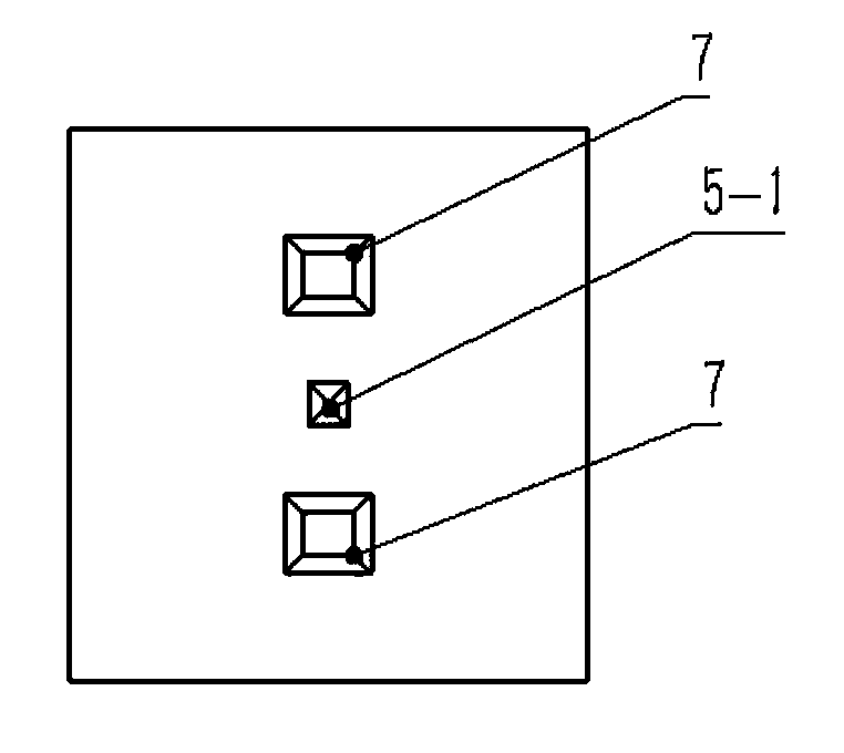
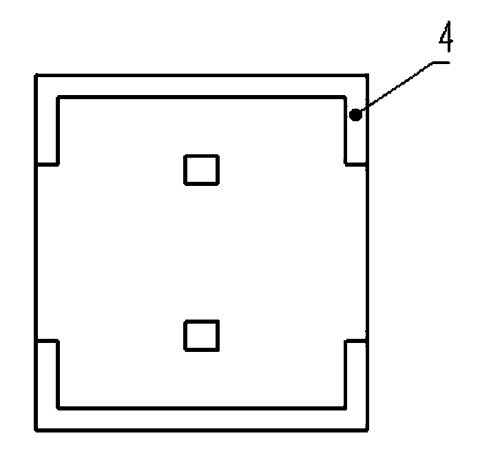
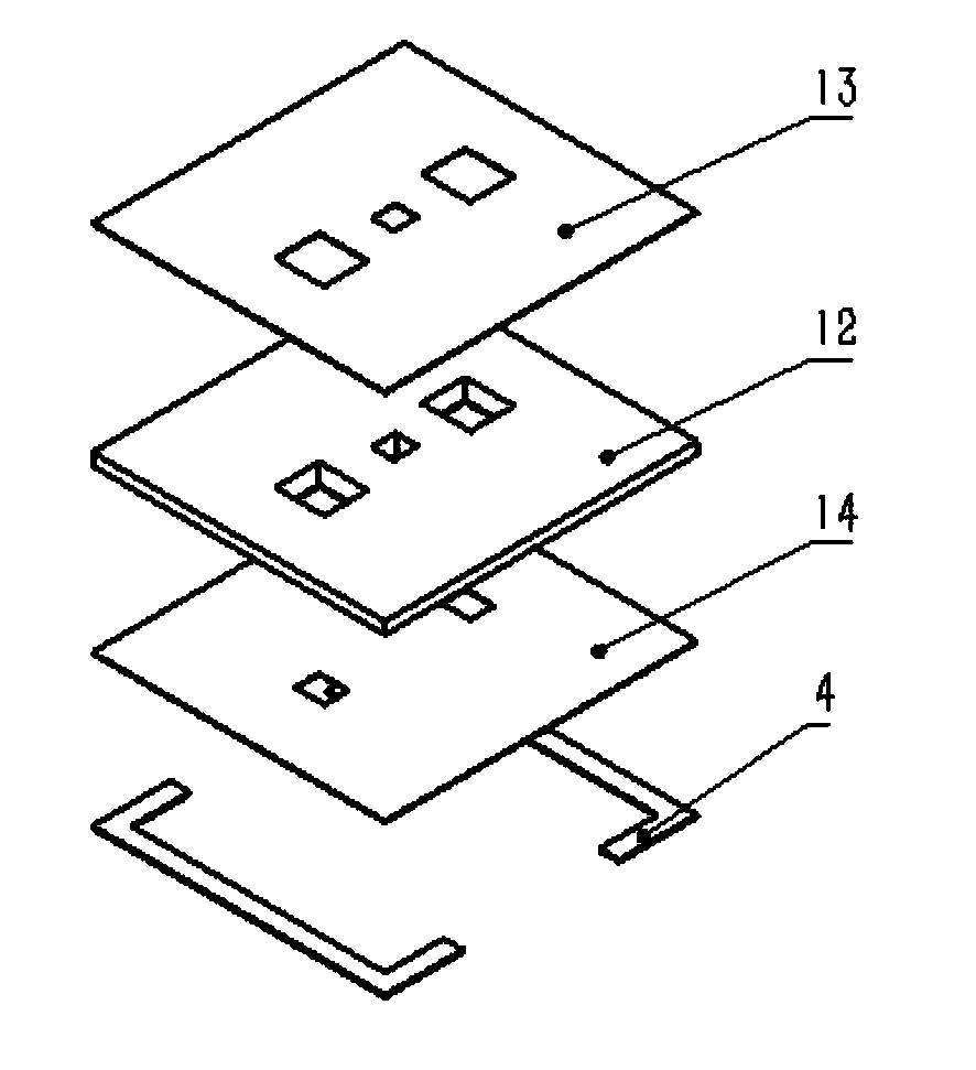
[0140] according to Figure 1-Figure 8 structure, the fabrication of the following chip was carried out. Among them, 1 is the in-situ electrothermal coupling chip of the transmission electron microscope; 2 is the top piece; 3 is the bottom piece; 4 is the metal bonding layer; 5 is the center window; 5-1 is the center window of the top piece; 5-2 is the center window of the bottom piece ; 7 is a sample injection port; 8 is a heating layer; 9 is a heating wire; 10 is the central area of ​​the heating wire; 11 is four contact electrodes (for heating); 12 is a silicon substrate; 13 is silicon nitride or silicon oxide Layer 1; 14 is a silicon nitride or silicon oxide layer 1'; 15 is an electrode material layer; 15-1 is a working electrode; 15-2 is a reference electrode; 15-3 is a counter electrode; 16 is a transition layer; 17 is Insulation layer; 18 is silicon nitride or ...

Embodiment 2

[0165] The gold nanoparticle colloidal solution sample is injected into the central window through the sample injection port of the in-situ electrothermal coupling chip of the transmission electron microscope obtained in Example 1, and put into the transmission electron microscope after packaging for observation. It is found that after the heating wire is heated, the nanometer particles can It is stable for a long time, and the shooting picture is very stable when heated in the electron microscope, which shows that the drift rate of the in-situ electrothermal coupling chip for the transmission electron microscope of the present invention is low.

Embodiment 3

[0167] The platinum nanoparticles were injected into the central window through the sample injection port of the in-situ electrothermal coupling chip obtained in Example 1, packaged and put into the transmission electron microscope for observation, and it was found that the two-dimensional arrangement of the atomic structure of the nanoparticles could be clearly seen. The lattice fringes indicate that the imaging resolution of the in-situ electrothermal coupling chip of the transmission electron microscope of the present invention can reach atomic-level resolution.


PUM

PropertyMeasurementUnit
sizeaaaaaaaaaa
sizeaaaaaaaaaa
thicknessaaaaaaaaaa

Abstract

The invention discloses a transmission electron microscope in-situ electrothermal coupling chip and a preparation method thereof. The structure is that an upper sheet and a lower sheet are combined through a metal bonding layer and are self-sealed to form an ultrathin chamber; both the upper sheet and the lower sheet are made of silicon substrates with silicon nitride or silicon oxide on two sides, and the upper sheet is provided with two sample injection ports and a central window; the lower sheet is provided with an electrode material layer, a transition layer, a silicon nitride or silicon oxide layer, a heating layer, an insulating layer, a silicon nitride or silicon oxide layer, a silicon substrate, a silicon nitride or silicon oxide layer and a central window, the central window is located in the center of the lower sheet, the heating layer is provided with four contact electrodes and an annular heating wire, the four contact electrodes are arranged on the edge of the chip, the heating wire is formed by communicating the tail ends of a plurality of arc lines, a slit is reserved when the arc lines are connected, and a working electrode in the electrode material layer is arranged at the slit and the front end of the working electrode extends out of the center window. The chip has the advantages of high resolution and low sample drift rate.

Description

technical field [0001] The invention relates to the field of electrothermal coupling chips, in particular to an in-situ electrothermal coupling chip for a transmission electron microscope and a preparation method thereof. Background technique [0002] The purpose of the present invention is to provide a transmission electron microscope in-situ electrothermal coupling chip that solves the limitation of the single function of the current in-situ chip. The role of electric-thermal coupling broadens the application range of in-situ heating chips or electrochemical chips. A single-function electrochemical chip or heating chip can only be used for electrochemical or heating chemical reactions. For some materials with poor conductivity, heating can increase their conductivity and cause reactions. For example, the conductivity of a polymer ion conductor at room temperature is 10 -3 -10 - 4 uS / cm level, but if the temperature rises to 60°C, its conductivity increases sharply. In...

Claims


Application Information

Patent Timeline
Patent Type & Authority Applications(China)
IPC IPC(8): H01J37/26G01N23/04G01N23/20G01N25/00G01N27/26
CPCG01N23/04G01N23/20G01N25/00G01N27/26H01J37/261
Inventor 廖洪钢
Owner XIAMEN CHIP NOVA TECH CO LTD
Why Eureka
Try Eureka