Doping method of silicon carbide component and preparation method thereof

A technology of components and silicon carbide, which is applied in the doping method of silicon carbide components and its preparation field, can solve the problems of damage and low ion activation rate, so as to improve the activation rate, deeply implant doping, and prevent the original atomic The effect of evaporation

Inactive Publication Date: 2020-06-30
江苏长晶科技股份有限公司
View PDF7 Cites 2 Cited by
  • Summary
  • Abstract
  • Description
  • Claims
  • Application Information

AI Technical Summary

Problems solved by technology

If the implanted ions reach a deep implanted area in the SiC material, the implanted energy may need to reach the MeV level. However, high-energy ion implanted will cause serious damage to the material surface in the implanted area, and the implanted ion activation rate is low.

Method used


Image

  • Doping method of silicon carbide component and preparation method thereof

Examples


Embodiment Construction

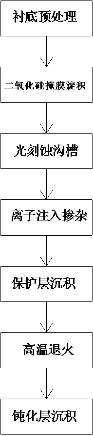
[0028] Below will be combined with the appended in the embodiment of the present invention figure 1 , clearly and completely describe the technical solutions in the embodiments of the present invention, obviously, the described embodiments are only some of the embodiments of the present invention, not all of them. Based on the embodiments of the present invention, all other embodiments obtained by persons of ordinary skill in the art without making creative efforts belong to the protection scope of the present invention.

[0029] The present invention provides such figure 1 A method of doping silicon carbide components and its preparation method shown in , comprising the following steps:

[0030] S1. Provide a semiconductor substrate, and pretreat the semiconductor substrate. Before pretreating the semiconductor substrate, protect the semiconductor substrate with protective wax, and Grinding and thinning is carried out, and the obtained semiconductor substrate structure is w...


PUM


Abstract

The invention discloses a doping method of a silicon carbide component and a preparation method of the silicon carbide component. The method comprises the following steps: S1, providing a semiconductor substrate, carrying out pretreatment on the semiconductor substrate; S2, growing an epitaxial layer on a surface of the pretreated semiconductor substrate, and depositing a silicon dioxide mask witha certain thickness on an outer surface of the epitaxial layer, S3, etching the silicon dioxide mask and forming a trench with a preset depth-to-width ratio such that a region needing to be doped isexposed; and S4, carrying out N times of ion implantation doping on the exposed doped region by using aluminum ions and nitrogen ions. Different implantation temperatures can be selected according todifferent ion implantation energies and different ion implantation dosages, and a uniform implantation structure is formed after multiple times of implantation such that the ion implantation damage isreduced, and the activation rate of implanted ions is improved.

Description

technical field [0001] The invention belongs to the technical field of semiconductor components, and in particular relates to a method for doping silicon carbide components and a preparation method thereof. Background technique [0002] Silicon carbide material has excellent physical and electrical properties. With its unique advantages such as wide band gap, high thermal conductivity, large saturation drift velocity and high critical breakdown electric field, it has become a high-power, high-frequency, durable Ideal semiconductor material for high temperature, radiation hardened devices. The breakdown voltage of silicon carbide power electronic devices can reach ten times that of silicon devices, and the on-resistance is only one tenth of that of silicon devices. The switching speed is fast, the thermal conductivity is high, the power conversion loss is small, and the heat dissipation system is simple. Ultimately, the volume and weight of the entire system are significantl...

Claims


Application Information

Patent Timeline
Patent Type & Authority Applications(China)
IPC IPC(8): H01L21/265H01L21/266H01L21/324
CPCH01L21/265H01L21/26506H01L21/266H01L21/324
Inventor 杨国江范荣定于世珩陈炜刘健夏昊天葛海波徐初惠杨灿灿孙冰冰
Owner 江苏长晶科技股份有限公司
Why Eureka
Try Eureka