Silicon carbide MOSFET device and preparation method thereof

A silicon carbide, N-JFET technology, used in semiconductor/solid-state device manufacturing, semiconductor devices, electrical components, etc., can solve problems such as current limiting capability, sudden change in electric field, and hidden reliability problems, and improve resistance to voltage shocks. , the effect of improving the current conduction capability and optimizing the current transmission path

Inactive Publication Date: 2019-03-12
INST OF MICROELECTRONICS CHINESE ACAD OF SCI +1
View PDF13 Cites 2 Cited by
  • Summary
  • Abstract
  • Description
  • Claims
  • Application Information

AI Technical Summary

Problems solved by technology

[0004] However, the current SiC MOSFET preparation method requires four ion implantations in the N-JFET region, P well region, P+ source region, and N+ source region in order to form the front structure, and the preparation process is cumbersome.
The P well is formed by implantation. High-energy ion implantation has an adverse effect on the surface roughness, causing increased surface scattering at the channel position, reducing the mobility of the inversion layer, and limiting the improvement of current capability.
The concentration of the drift layer and the buffer layer varies greatly, which makes the electric field of the device suddenly change during operation, and there are hidden dangers in reliability

Method used


Image

  • Silicon carbide MOSFET device and preparation method thereof
  • Silicon carbide MOSFET device and preparation method thereof
  • Silicon carbide MOSFET device and preparation method thereof

Examples


Embodiment Construction

[0038] In order to make the object, technical solution and advantages of the present invention clearer, the present invention will be further described in detail below in conjunction with specific embodiments and with reference to the accompanying drawings.

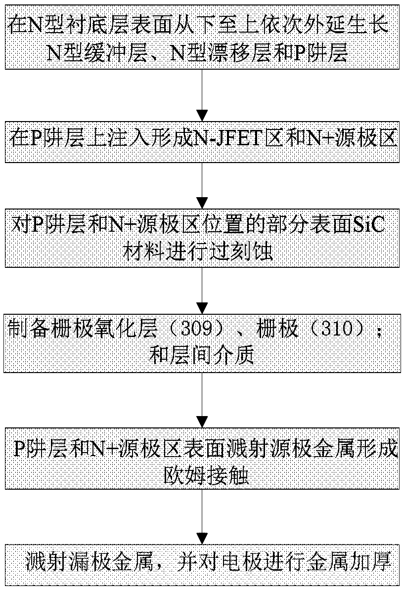
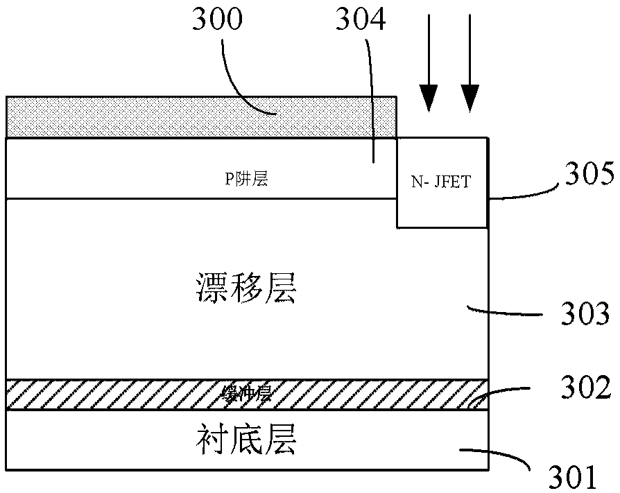
[0039] According to an embodiment of the present invention, a method for preparing a silicon carbide MOSFET is provided, such as figure 2 shown, including:

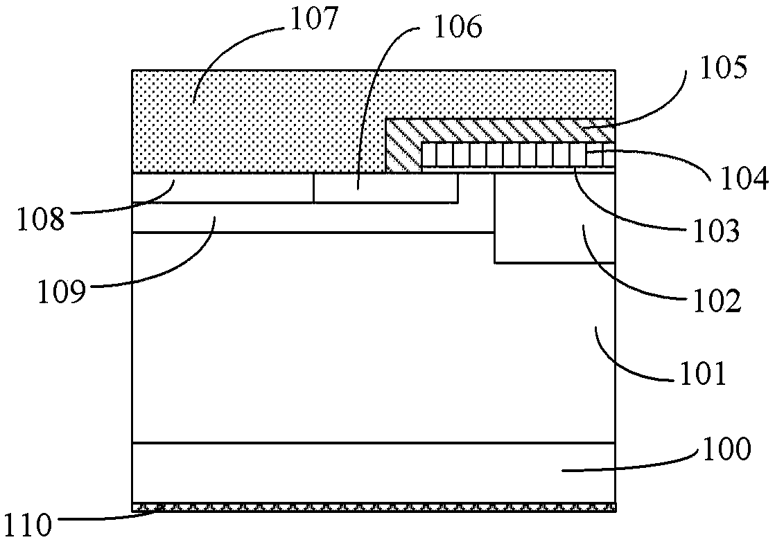
[0040] Over-etching the SiC material on the part of the surface of the P well layer 304 and the N+ source region 306;

[0041] The source contact window is etched, and the source metal 312 is sputtered on the surface of the P well layer 304 and the N+ source region 306 to form an ohmic contact.

[0042] Wherein, in the P well layer 304, the middle area of ​​the P well concentration is the highest, and gradually decreases toward both sides. If it is not etched away, the concentration of the P well surface area is not enough to form an ohmic contact. Concentrated P+...


PUM


Abstract

The invention provides a silicon carbide MOSFET device and a preparation method thereof, and relates to the field of semiconductor manufacturing. The preparation method comprises: over-etching SiC material on a partial surface at a P-well layer and an N+ source region; and etching a source contact window, and sputtering the source metal on the surface of the P-well layer and the N+ source region to form an ohmic contact. In the invention, by etching the surface of the P-well layer, the high-concentration P-well region can be directly in ohmic contact with the source metal, which optimizes thecurrent transmission path, and does not require high-dose P+ injection, reduces injection damage, and reduces preparation cost.

Description

technical field [0001] The invention relates to the field of semiconductor manufacturing, in particular to a silicon carbide MOSFET device and a preparation method. Background technique [0002] Silicon carbide (SiC) is an ideal semiconductor material for high voltage, high frequency and high temperature applications. This is mainly due to the large critical electric field of SiC (10 times higher than Si), large bandgap (3 times that of Si), large thermal conductivity (4 times that of Si), and large electron saturation velocity (twice that of Si). times). These characteristics make SiC replace Si to manufacture MOSFET devices, which can improve carrier mobility, reduce channel on-resistance, and improve short-channel effect. [0003] figure 1 Shown is the current typical planar gate SiC MOSFET structure, including: 100 substrate layer, 101 drift layer, 102N-JFET region, 103 gate oxide, 104 polysilicon gate, 105 interlayer dielectric, 106N+ source, 107 source metal, 108P+ ...

Claims


Application Information

Patent Timeline
Patent Type & Authority Applications(China)
IPC IPC(8): H01L21/336H01L21/28H01L29/78H01L29/45
CPCH01L29/401H01L29/45H01L29/66068H01L29/7828
Inventor 陈宏宁文果韩忠霖冯奇
Owner INST OF MICROELECTRONICS CHINESE ACAD OF SCI
Why Eureka
Try Eureka