Hexagonal boron nitride with isoelectronic doping of phosphorus, and preparation method thereof
A technology of hexagonal boron nitride and isoelectronics is applied in the field of materials to achieve the effect of simple preparation process
- Summary
- Abstract
- Description
- Claims
- Application Information
AI Technical Summary
Problems solved by technology
Method used
Image
Examples
Embodiment 1
[0051] Experimental steps:
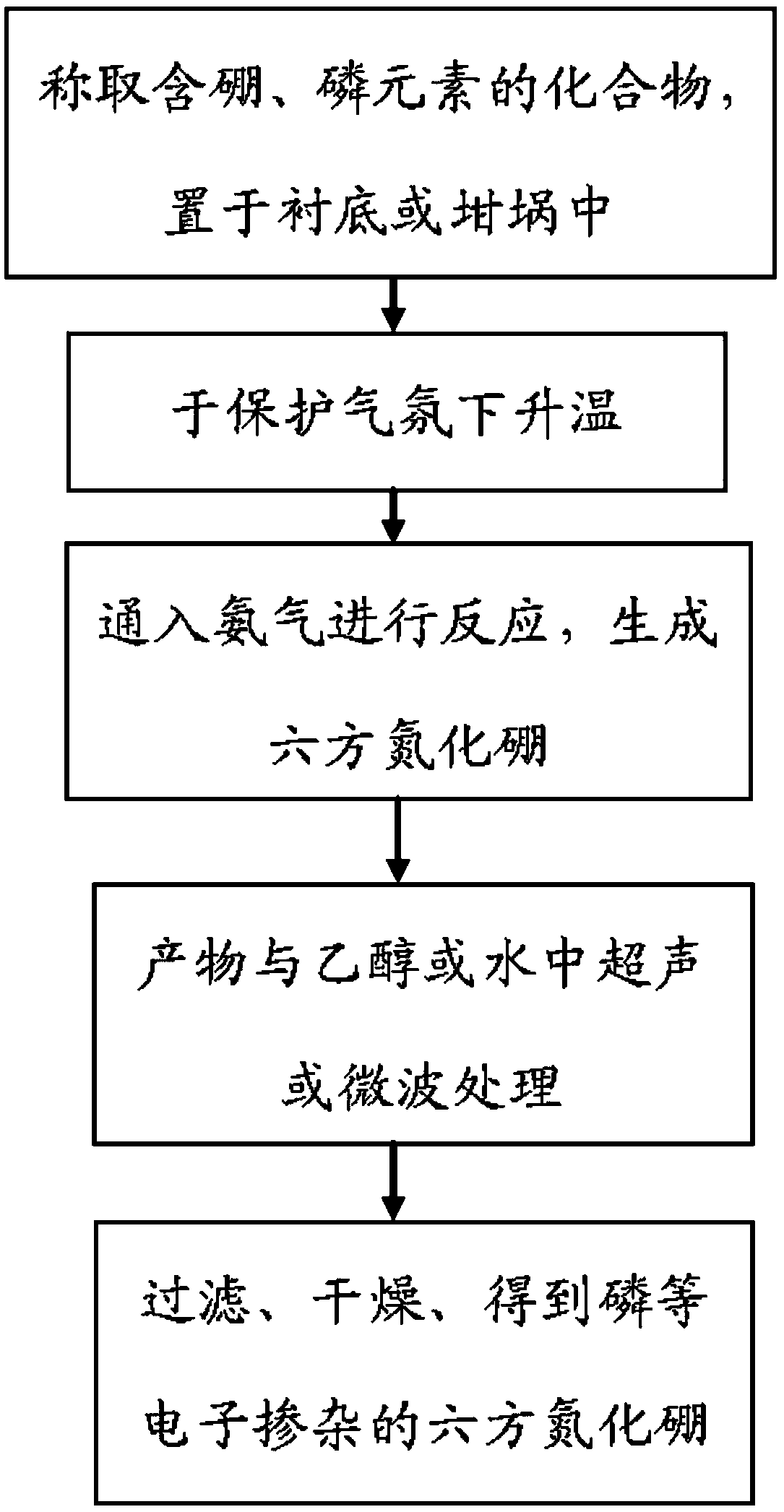
[0052]Weigh 2 g of boron phosphate powder and place it in an alumina crucible. Under an argon atmosphere of 300 sccm, the temperature was raised to 1000 °C at a rate of 10 °C / min, and annealed at 1000 °C for 10 min. Afterwards, ammonia gas was introduced at a rate of 50 sccm, and reacted at 1000° C. for 30 minutes. After naturally cooling down to room temperature, the product was taken out, ultrasonically treated in ethanol, filtered and dried to obtain the hexagonal boron nitride doped with electrons such as phosphorus.
[0053] Result analysis:
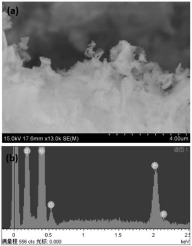
[0054] figure 2 (a) is the microscopic morphology of the electron-doped hexagonal boron nitride such as phosphorus obtained in Example 1, which can be seen to be a two-dimensional nanosheet structure; figure 2 In (b), the peak of P element can be clearly seen, indicating that P element is also involved in the formation of BN, and P-doped hexagonal boron nitride is obtained.
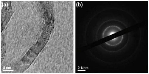
[0055] image 3 (a) ...
Embodiment 2
[0064] Experimental steps:
[0065] Weigh 2 g of boron phosphate powder, place it in an alumina crucible, raise the temperature to 1100 °C at a rate of 10 °C / min under an argon atmosphere of 300 sccm, and heat-preserve and anneal at 1100 °C for 10 min. Afterwards, ammonia gas was introduced at a rate of 50 sccm, and reacted at 1100° C. for 30 minutes. After naturally cooling down to room temperature, the product was taken out, ultrasonically treated in ethanol, filtered and dried to obtain the hexagonal boron nitride doped with electrons such as phosphorus.
[0066] Result analysis:
[0067] from Figure 9 (a) is the microscopic appearance of electron-doped hexagonal boron nitride such as phosphorus obtained in embodiment 2, and it can still be seen that it is a two-dimensional nanosheet structure; Figure 9 In (b), the peak of P element can be clearly seen, indicating that P-doped hexagonal boron nitride has been obtained.
[0068] from Figure 10 (a) It can be seen that...
Embodiment 3
[0070] Experimental steps:
[0071] Weigh 2 g of boron phosphate powder, place it in an alumina crucible, raise the temperature to 1180 °C at a rate of 10 °C / min under an argon atmosphere of 300 sccm, and heat-preserve and anneal at 1180 °C for 10 min. Afterwards, ammonia gas was introduced at a rate of 50 sccm, and the reaction was carried out at 1180°C for 30 minutes. After naturally cooling down to room temperature, the product was taken out, ultrasonically treated in ethanol, filtered and dried to obtain the hexagonal boron nitride doped with electrons such as phosphorus.
[0072] Result analysis:
[0073] from Figure 11 (a) is the microscopic morphology of the electron-doped hexagonal boron nitride such as phosphorus obtained in Example 3, and it can be seen that the two-dimensional nanosheet structure is agglomerated in a circular shape; Figure 11 In (b), the peak of P element can be clearly seen, indicating that P-doped hexagonal boron nitride has been obtained.
...
PUM
 Abstract
Description
Claims
Application Information
 - R&D
- Intellectual Property
- Life Sciences
- Materials
- Tech Scout
- Unparalleled Data Quality
- Higher Quality Content
- 60% Fewer Hallucinations
Browse by: Latest US Patents, China's latest patents, Technical Efficacy Thesaurus, Application Domain, Technology Topic, Popular Technical Reports.
© 2025 PatSnap. All rights reserved.Legal|Privacy policy|Modern Slavery Act Transparency Statement|Sitemap|About US| Contact US: help@patsnap.com


