Method of measuring impurity activation energy in semiconductor

An activation energy and semiconductor technology, applied in the direction of single semiconductor device testing, measuring electricity, measuring devices, etc., can solve the problems of large amount of calculation, high cost, complex testing system, etc., to reduce the experimental cost, improve the computing efficiency, and simplify the process. Effect

Active Publication Date: 2020-07-03
SOUTH UNIVERSITY OF SCIENCE AND TECHNOLOGY OF CHINA
View PDF8 Cites 2 Cited by
  • Summary
  • Abstract
  • Description
  • Claims
  • Application Information

AI Technical Summary

Problems solved by technology

(1) Electricity test For example, the activation energy of impurities in semiconductors can be measured by variable temperature Hall experiment. However, the inventors have found that this method requires relatively high conductivity of materials, and electrodes need to be made. The obtained experimental results are often subject to various influences. Influenced by factors, the error is relatively large
Deep level transient spectroscopy can also measure the activation energy of impurities introduced into the deep level in semiconductors, but it needs to make Schottky junction or pn junction d

Method used


Image

  • Method of measuring impurity activation energy in semiconductor
  • Method of measuring impurity activation energy in semiconductor
  • Method of measuring impurity activation energy in semiconductor

Examples


Embodiment Construction

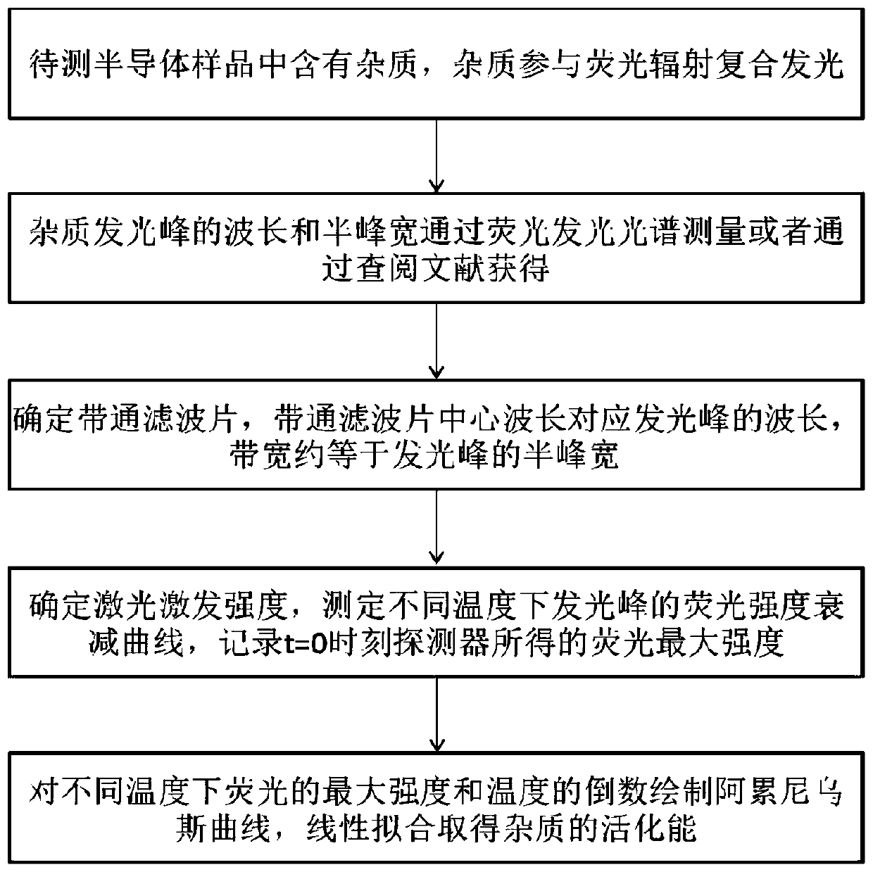
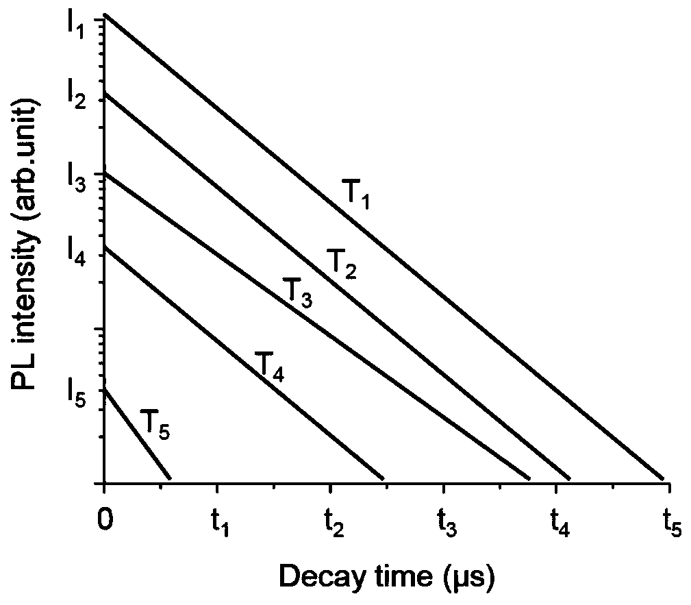
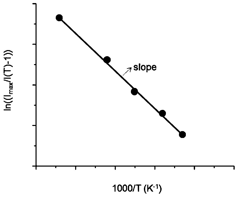
[0027] In order to make the purpose, technical solutions and advantages of the embodiments of the present invention more clear, various implementation modes of the present invention will be described in detail below in conjunction with the accompanying drawings. However, those of ordinary skill in the art can understand that, in each implementation manner of the present invention, many technical details are provided for readers to better understand the present application. However, even without these technical details and various changes and modifications based on the following implementation modes, the technical solution claimed in this application can also be realized. The division of the following embodiments is for the convenience of description, and should not constitute any limitation to the specific implementation of the present invention, and the various embodiments can be combined and referenced to each other on the premise of no contradiction.

[0028] The technical ...


PUM


Abstract

The embodiment of the invention relates to a semiconductor material analysis and detection technology, discloses a method for measuring activation energy of impurities in a semiconductor, and expandsapplication occasions of a time-resolved fluorescence spectrum. The method comprises the following steps of impurities in the semiconductor participating in fluorescence radiation composite luminescence; obtaining the wavelength and the half-peak width of an impurity luminescence peak; determining a band-pass filter, determining laser excitation intensity, determining fluorescence intensity attenuation curves of corresponding light-emitting peaks at different temperatures, and recording the maximum fluorescence intensity obtained by the detector at the moment t=0; drawing an Arrhenius curve according to the fluorescence maximum intensity and the reciprocal of the temperature measured by the detector at different temperatures, carrying out linear fitting to obtain a slope, and multiplying the slope by a Boltzmann constant to obtain the activation energy of the impurities. The method is advantaged in that the temperature-dependent carrier lifetime information can be obtained by using thevariable-temperature time-resolved fluorescence spectrum, the activation energy of an impurity introduction energy level can be obtained, the method is simple, convenient and easy to operate, experiment cost is greatly reduced, and operation efficiency is greatly improved.

Description

technical field [0001] The embodiments of the present invention relate to the technical field of analysis and detection of semiconductor materials, and in particular to a method for measuring the activation energy of impurities in semiconductors. Background technique [0002] The impurity activation energy (or ionization energy) in semiconductor is an important conductance physical parameter of doped semiconductor, which is crucial to the performance of semiconductor materials and devices. [0003] There are usually two methods of obtaining the activation energy of impurities in semiconductors: electrical and optical. (1) Electricity test For example, the activation energy of impurities in semiconductors can be measured by temperature-variable Hall experiments. However, the inventors have found that this method requires relatively high conductivity of materials, and electrodes need to be fabricated. The obtained experimental results are often subject to various influences. ...

Claims


Application Information

Patent Timeline
IPC IPC(8): G01R31/265G01N21/64
CPCG01R31/2656G01R31/2601G01N21/6408G01N21/6489
Inventor 杨安丽张新河高博陈施施温正欣张志新张国旗
Owner SOUTH UNIVERSITY OF SCIENCE AND TECHNOLOGY OF CHINA
Why Eureka
Try Eureka