Semiconductor device

A semiconductor and nitride semiconductor technology, applied in semiconductor devices, semiconductor/solid-state device manufacturing, semiconductor/solid-state device components, etc., and can solve problems such as inapplicability to power equipment

Active Publication Date: 2020-07-03
ROHM CO LTD
View PDF6 Cites 0 Cited by
  • Summary
  • Abstract
  • Description
  • Claims
  • Application Information

AI Technical Summary

Problems solved by technology

[0005] However, in order to be used as a power device, it needs to be a normally-off device that blocks current at zero bias, and HEMTs as described above are not suitable for power devices

Method used


Image

  • Semiconductor device
  • Semiconductor device
  • Semiconductor device

Examples


no. 1 example

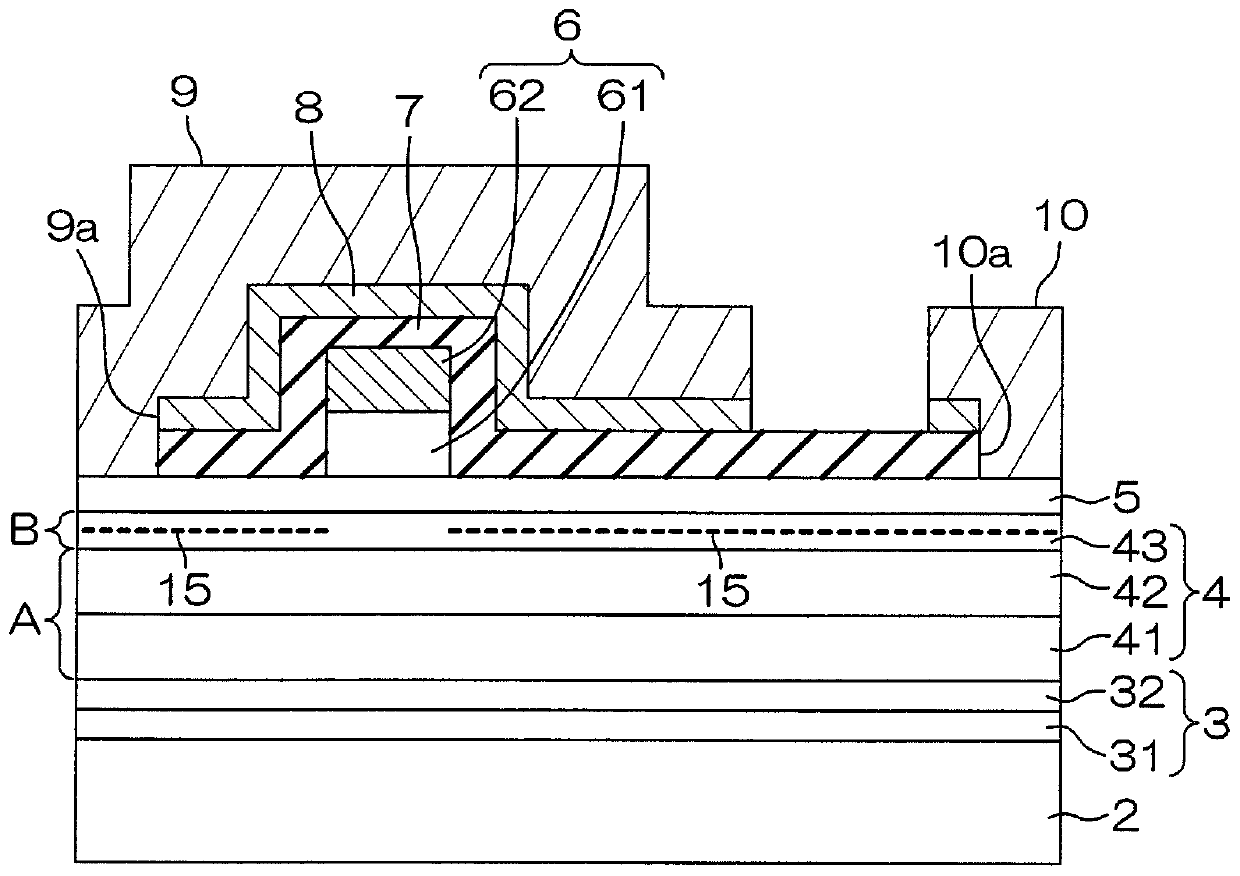
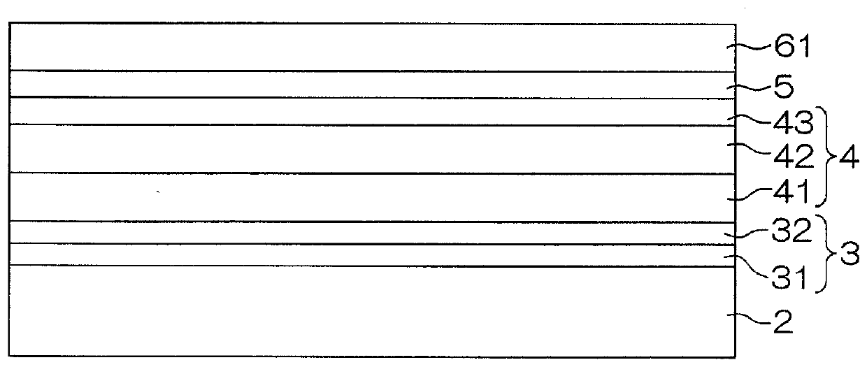
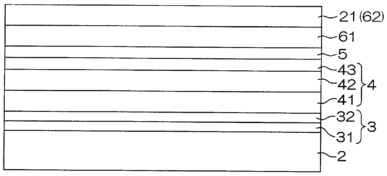
[0085] In the first embodiment, the acceptor type impurity of the first nitride semiconductor layer 41 is Mg (magnesium). The acceptor density N of the first nitride semiconductor layer 41 T with donor density N D The difference (N T ﹣N D ) is 5×10 17 cm -3 . The acceptor energy level E of the first nitride semiconductor layer 41 T and the energy E at the top of the valence band V The difference (E T ﹣E V ) is 0.2eV.

[0086] On the other hand, the acceptor type impurity of the second nitride semiconductor layer 42 is C (carbon). The acceptor density N of the second nitride semiconductor layer 42 T with donor density N D The difference (N T ﹣N D ) is 4×10 16 cm -3 . The acceptor energy level E of the second nitride semiconductor layer 42 T and the energy E at the top of the valence band V The difference (E T ﹣E V ) is 0.9eV.

[0087] That is, the acceptor density N of the first nitride semiconductor layer 41 T with donor density N D The difference (N T...

no. 3 example

[0092] In the third embodiment, the acceptor type impurity of the first nitride semiconductor layer 41 is Mg (magnesium). The acceptor density N of the first nitride semiconductor layer 41 T with donor density N D The difference (N T ﹣N D ) is 5×10 17 cm -3 . The acceptor energy level E of the first nitride semiconductor layer 41 T and the energy E at the top of the valence band V The difference (E T ﹣E V ) is 0.2eV.

[0093] On the other hand, the acceptor type impurity of the second nitride semiconductor layer 42 is Fe (iron). The acceptor density N of the second nitride semiconductor layer 42 T with donor density N D The difference (N T ﹣N D ) is 4×10 16 cm -3 . The acceptor energy level E of the second nitride semiconductor layer 42 T and the energy E at the top of the valence band V The difference (E T ﹣E V ) is 2.8eV.

[0094] [4] Fourth embodiment

[0095] In the fourth embodiment, the acceptor impurity of the first nitride semiconductor layer 41 ...


PUM

PropertyMeasurementUnit
thicknessaaaaaaaaaa
thicknessaaaaaaaaaa
thicknessaaaaaaaaaa

Abstract

A semiconductor device 1 includes a substrate 2, an electron transit layer 4 disposed on the substrate 2, and an electron supply layer 5 disposed on the electron transit layer 4. The electron transitlayer 4 includes: a conductive path forming layer 43 that is in contact with the electron supply layer 5; a first semiconductor region (first nitride semiconductor layer) 41 that contains an acceptor-type impurity; and a second semiconductor region (second nitride semiconductor layer) 42 that is disposed at a position closer to the conductive path forming layer 43 than is the first semiconductor region 41, the second semiconductor region 42 containing anacceptor-type impurity. The acceptor density of the first semiconductor region 41 is greater than the acceptor density of the second semiconductor region 42.

Description

technical field [0001] The present invention relates to a semiconductor device, for example, to a nitride semiconductor device formed of a group III nitride semiconductor (hereinafter sometimes simply referred to as "nitride semiconductor"). Background technique [0002] The group III nitride semiconductor refers to a semiconductor using nitrogen as a group V element among group III-V semiconductors. Typical examples are aluminum nitride (AlN), gallium nitride (GaN), and indium nitride (InN). Generally can be expressed as Al x In y Ga 1-x-y N (0≦x≦1, 0≦y≦1, 0≦x+y≦1). [0003] A HEMT (High Electron Mobility Transistor; High Electron Mobility Transistor) using such a nitride semiconductor has been proposed. Such a HEMT includes, for example, an electron transport layer formed of GaN and an electron supply layer formed of epitaxially grown AlGaN on the electron transport layer. A pair of source and drain electrodes are formed so as to be in contact with the electron suppl...

Claims


Application Information

Patent Timeline
Patent Type & Authority Applications(China)
IPC IPC(8): H01L21/338H01L21/337H01L29/778H01L29/808H01L29/812
CPCH01L29/7786H01L29/2003H01L29/402H01L29/1066H01L29/207H01L29/66462H01L29/42316H01L23/535H01L29/7787
Inventor 田中岳利
Owner ROHM CO LTD
Why Eureka
Try Eureka