Mask plate and exposure method

An exposure method and mask technology, which are applied in the field of semiconductor manufacturing, can solve the problems of limited exposure field of view and reduced exposure efficiency.

Active Publication Date: 2020-07-07
SHANGHAI MICRO ELECTRONICS EQUIP (GRP) CO LTD
View PDF7 Cites 5 Cited by
  • Summary
  • Abstract
  • Description
  • Claims
  • Application Information

AI Technical Summary

Problems solved by technology

In the process of making PSS graphics, due to the limited size of the field of view of a single exposure, in order to form the entire piece of PSS graphics, it is necessary to use the method of splicing exposure. The existing method of splicing area division is as follows: figure 1 As shown (orthogonal line division), the stitching line in the figure is a virtual line and will not be actually imaged. The stitching area may need to use 4 exposure fields to complete, such as figure 2 shown
In this solution, the graphic line width of the exposure area at the splicing point will be halved, resulting in higher resolution and higher requirements for image quality, so it is often necessary to reduce the exposure field of view to meet the image quality requirements, but the exposure The exposure efficiency will be greatly reduced when the field of view is reduced

Method used


Image

  • Mask plate and exposure method
  • Mask plate and exposure method
  • Mask plate and exposure method

Examples


Embodiment Construction

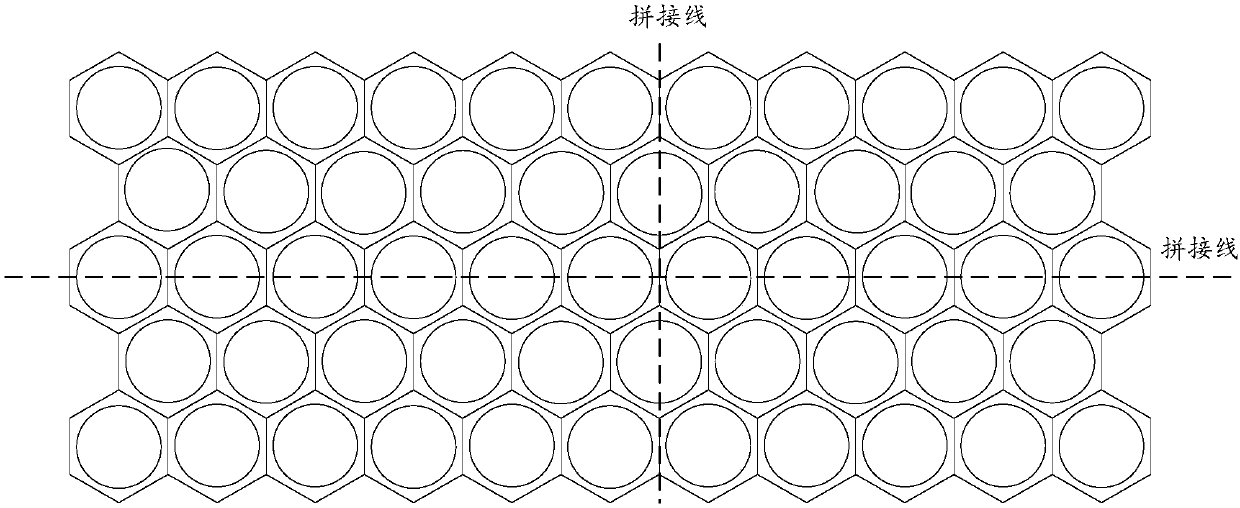
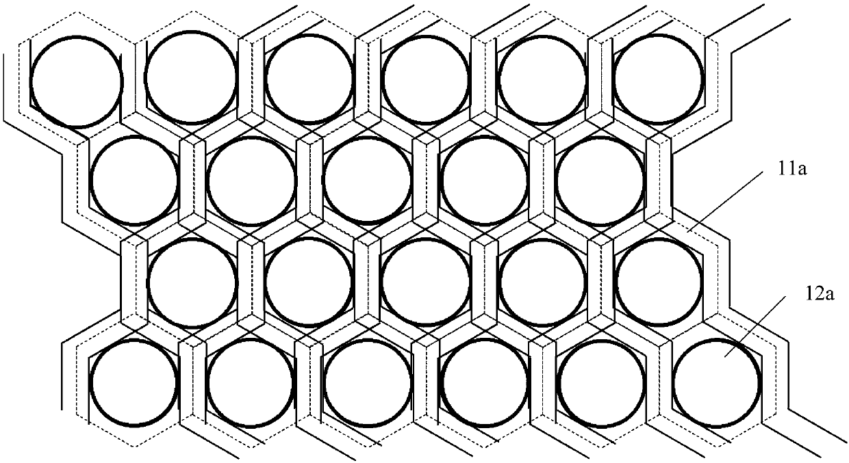
[0041] Such as image 3 As shown, the PSS pattern is a plurality of hexagons arranged in a honeycomb shape, the circular part protrudes to form a protruding part 12a, and the rest part is recessed downward to form a concave part 11a, and several protruding parts 12a are independent of each other, and each The protrusions 12a are all surrounded by the recesses 11a. When preparing the PSS pattern, the protruding portion 12a corresponds to the non-exposed area, and the depressed portion 11a corresponds to the exposed area. The inventors found that the exposure area of ​​the PSS pattern can be disassembled into two groups of line mirror symmetrical figures, and the boundary of each set of figures is the tangent line of the circular non-exposed area, so the overlapping exposure method can be used to form the PSS figure.

[0042] Based on this, the present invention provides a mask plate and an exposure method, including a complementary first mask pattern and a second mask pattern,...


PUM


Abstract

The invention provides a mask plate and an exposure method. The mask plate comprises a first mask pattern and a second mask pattern which are complementary, wherein the first mask pattern comprises aplurality of first strip-shaped patterns extending along a first direction; the second mask pattern comprises a plurality of second strip-shaped patterns extending along a second direction; the firstdirection is crossed with the second direction; in the exposure method, the first mask pattern and the second mask pattern are employed respectively to sequentially execute twice exposure processes onthe LED substrate, so that after alignment overlapping of the formed exposure patterns, a PSS pattern can be generated; compared with a traditional splicing mode, the method has the advantages that the line widths of all the pattern areas are consistent, so that the requirement for image quality is lowered, and an exposure view field does not need to be reduced.

Description

technical field [0001] The invention relates to the technical field of semiconductor manufacturing, in particular to a mask plate and an exposure method. Background technique [0002] Patterned Sapphire Substrate (PSS), that is, a mask for dry etching is grown on the sapphire substrate, a PSS pattern is formed by a standard photolithography process, the sapphire is etched by ICP etching technology, and the mask is removed , and then grow GaN material on it, so that the vertical epitaxy of the GaN material becomes lateral epitaxy, on the one hand, it can effectively reduce the dislocation density of the GaN epitaxial material, thereby reducing the non-radiative recombination of the active region and reducing the reverse leakage current , improve the life of the LED; on the other hand, the light emitted by the active area is scattered by the GaN and sapphire substrate interface multiple times, which changes the exit angle of the total reflection light and increases the probabi...

Claims


Application Information

Patent Timeline
Patent Type & Authority Applications(China)
IPC IPC(8): G03F1/00G03F7/20H01L33/20
CPCG03F1/00G03F7/2022G03F7/70475H01L33/20
Inventor 任书铭
Owner SHANGHAI MICRO ELECTRONICS EQUIP (GRP) CO LTD
Why Eureka
Try Eureka