
Microcontroller and manufacturing method thereof

A technology of a microcontroller and a manufacturing method, which is applied in the direction of transistors, etc., can solve the problems of long length, waste, and no layer in the back pass.

Active Publication Date: 2020-07-07
NINGBO SEMICON INT CORP
View PDF6 Cites 1 Cited by
  • Summary
  • Abstract
  • Description
  • Claims
  • Application Information

AI Technical Summary

Problems solved by technology

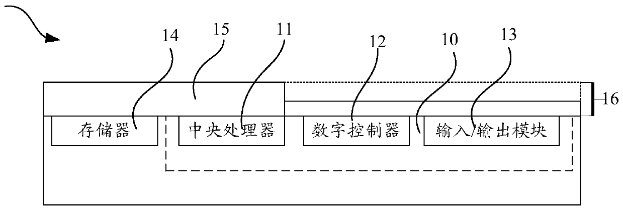
[0005] (1) The SoC process used by the MCU is the result of the process compatibility of the various modules contained in the MCU, but in fact there are great differences in the process of some modules. For details, please refer to Figure 1B , in MCU1, including central processing unit (logicCore) 11, logic controller (logic controller) 12, input / output module 13 and modules such as various interfaces and control algorithms) etc. logic part (logic) 10 process and instruction memory The process is very different. When the MCU 1 only has the logic part 10, the number of layers with the corresponding layout structure in the MCU1 is 28-30 layers (corresponding to 28-30 masks), and when the MCU 1 except the logic part 10. When there are other non-logic devices or modules, the number of layers with a corresponding layout structure in the MCU 1 will increase accordingly (that is, usually correspondingly increase 5 or more photomasks), for example, the logic part 10 After the instruction memory 14 is compatible, the number of layers with the corresponding layout structure in the MCU 1 will change from about 30 layers to about 40 layers, and the added additional layer 15 has an electrical interconnection for electrically connecting the instruction memory 14 and the central processing unit 11. The connection structure (not shown, it can also be said to be wiring), that is, the number of masks for manufacturing the MCU1 will change from about 30 to about 40, resulting in a sharp increase in plate-making costs
[0006] (2) The layout layer added due to the different processes of some modules objectively leads to the fact that the back-channel layout layer on the top layer of some modules is often meaningless in the back-end interconnection process and does not require wiring, but in order to ensure the consistency of the process stability, it is necessary to add a large number of dummy structures (dummy) in the subsequent layer corresponding to these modules, and these dummy structures themselves are a waste of waste of materials and time, for example Figure 1B As shown, when the MCU1 only has the logic part 10, the number of layers with the corresponding layout structure is 28 layers. After the central processing unit 11 is compatible with the instruction memory, 5 layers are added in the MCU 1 with the corresponding layout structure of the subsequent process. (that is, the wiring that electrically connects the instruction memory 14 and the central processing unit 11) of the additional layer 15, at this time, the additional layer 15 (total thickness is the μm level) that increases is in the logic part 10 of the MCU 1 except the central processing unit 11 The module does not need, but due to the planar process, that is, additional layers 16 will be formed on the top of the modules other than the central processing unit 11 in the logic part 10, and the additional layers 16 will have the same number of layers and thickness as the additional layers 15 , and a large number of dummy structures (dummy, not shown) need to be placed in the additional layer 1, resulting in waste
[0007] (3) When the MCU is integrated in SoC mode, the lead wire between the instruction memory and the central processing unit is too long, which limits the improvement of the access speed of the instruction
Specifically, please refer to Figure 1B , because the MCU1 is integrated in an SoC manner, its instruction memory 14 needs to be distributed side by side with the central processing unit 11, that is, the instruction memory 14 is separately packaged outside the central processing unit 11, and then the instruction memory 14, the central processing unit 11, and the logic controller 12 1. On the input / output module 13, an electrical interconnection structure (not shown, usually including conductive contact plugs and metal interconnection wires) for realizing the electrical connection between the instruction memory 14 and the central processing unit 11 is manufactured, the electrical interconnection structure That is, it is formed in the additional layer 15. Obviously, the electrical interconnection structure includes a part (not shown) drawn vertically upward from the central processing unit 11, a part (not shown) drawn vertically upward from the instruction memory 14, and connections In the horizontal part (not shown) between these two parts, the length of the electrical interconnection structure is too long relative to the straight line segment between the two points of the instruction memory 14 and the central processing unit 11, thus causing the simplification of instructions. Read and store speeds are limited and cannot be further improved

Method used


Image

  • Microcontroller and manufacturing method thereof
  • Microcontroller and manufacturing method thereof
  • Microcontroller and manufacturing method thereof

Examples


Embodiment Construction

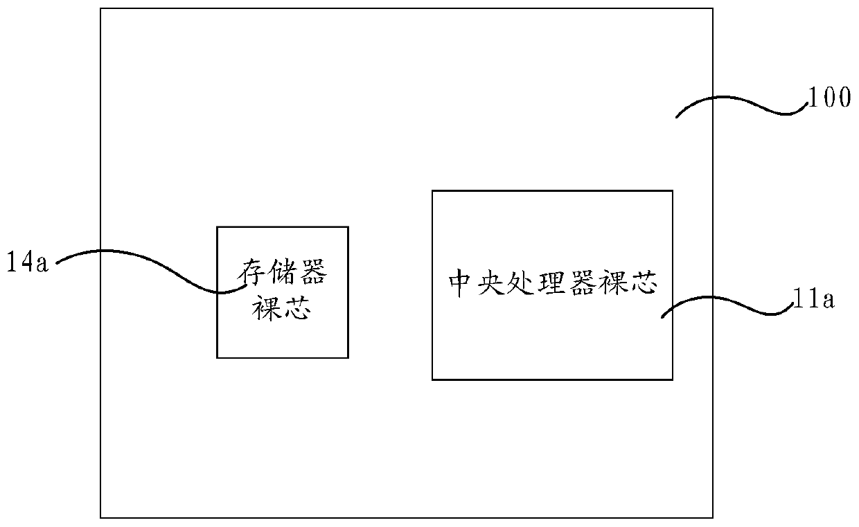
[0030] The technical solutions of the present invention will be described in further detail below in conjunction with the accompanying drawings and specific embodiments. The advantages and features of the present invention will become clearer from the following description. It should be noted that all the drawings are in a very simplified form and use imprecise scales, and are only used to facilitate and clearly assist the purpose of illustrating the embodiments of the present invention. Similarly, if a method described herein includes a series of steps, the order in which these steps are presented is not necessarily the only order in which these steps can be performed, and some described steps may be omitted and / or some not described herein Additional steps can be added to the method. If the components in a certain drawing are the same as those in other drawings, although these components can be easily identified in all the drawings, in order to make the description of the d...


PUM


Abstract

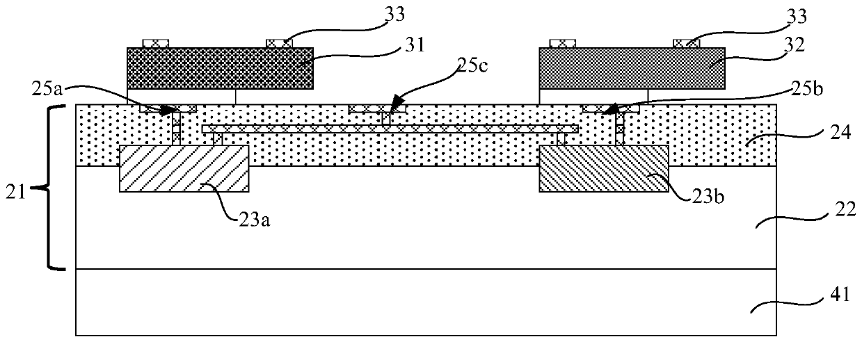
The invention provides a microcontroller and a manufacturing method thereof. The microcontroller comprises a logic control substrate, at least one memory bare chip and at least one non-memory bare chip, wherein the memory bare chips and the non-memory bare chips are arranged on the logic control substrate. The logic control substrate comprises a semiconductor device layer and an interconnection dielectric layer, a central processing unit and at least one logic controller are formed in the semiconductor device layer, all the memory bare cores are arranged on the interconnection dielectric layerside by side or in a stacked mode, and at least one memory bare core is electrically connected with the central processing unit through a corresponding electric interconnection structure in the interconnection dielectric layer; and all the non-memory bare cores are arranged on the interconnection dielectric layer side by side or in a stacked manner, and are electrically connected with the corresponding logic controllers through the corresponding electric interconnection structures in the interconnection dielectric layer. According to the invention, layouts and unnecessary virtual structures required in the manufacturing process stage of the integrated circuit device can be reduced, and the cost can be reduced.

Description

technical field [0001] The invention relates to the technical field of integrated circuit manufacturing, in particular to a microcontroller and a manufacturing method thereof. Background technique [0002] Microcontroller (Microcontroller Unit, MCU), also known as Single Chip Microcomputer (Single Chip Microcomputer) or single-chip microcomputer, is to appropriately reduce the frequency and specifications of the Central Processing Unit (Central Process Unit, CPU, also called logic core), And basic modules such as memory (Memory, which can also be called memory), counter (Timer), input / output (I / O) modules, various interfaces (such as Debug interface, USB interface) and other control algorithm modules, as well as MEMS Extended functional modules such as sensors or RF communication modules are integrated on a single chip to form a chip-level computer, which can be used for different combination controls for different applications. [0003] One way of making an MCU in the prio...

Claims


Application Information

Patent Timeline
IPC IPC(8): H01L27/108
CPCH10B12/00
Inventor 唐莹袁骁霖
Owner NINGBO SEMICON INT CORP
Learn More