Bootstrap sampling switch circuit, sample hold circuit and analog-to-digital converter

A bootstrap sampling switch, circuit technology, applied in the direction of analog-to-digital converter, analog-to-digital conversion, code conversion, etc., can solve the problem of long rise and fall time of the output clock

Pending Publication Date: 2020-07-07
SHANGHAI BEILING
View PDF4 Cites 5 Cited by
  • Summary
  • Abstract
  • Description
  • Claims
  • Application Information

AI Technical Summary

Problems solved by technology

[0012] The technical problem to be solved by the present invention is to provide a bo

Method used


Image

  • Bootstrap sampling switch circuit, sample hold circuit and analog-to-digital converter
  • Bootstrap sampling switch circuit, sample hold circuit and analog-to-digital converter
  • Bootstrap sampling switch circuit, sample hold circuit and analog-to-digital converter

Examples


Embodiment 1

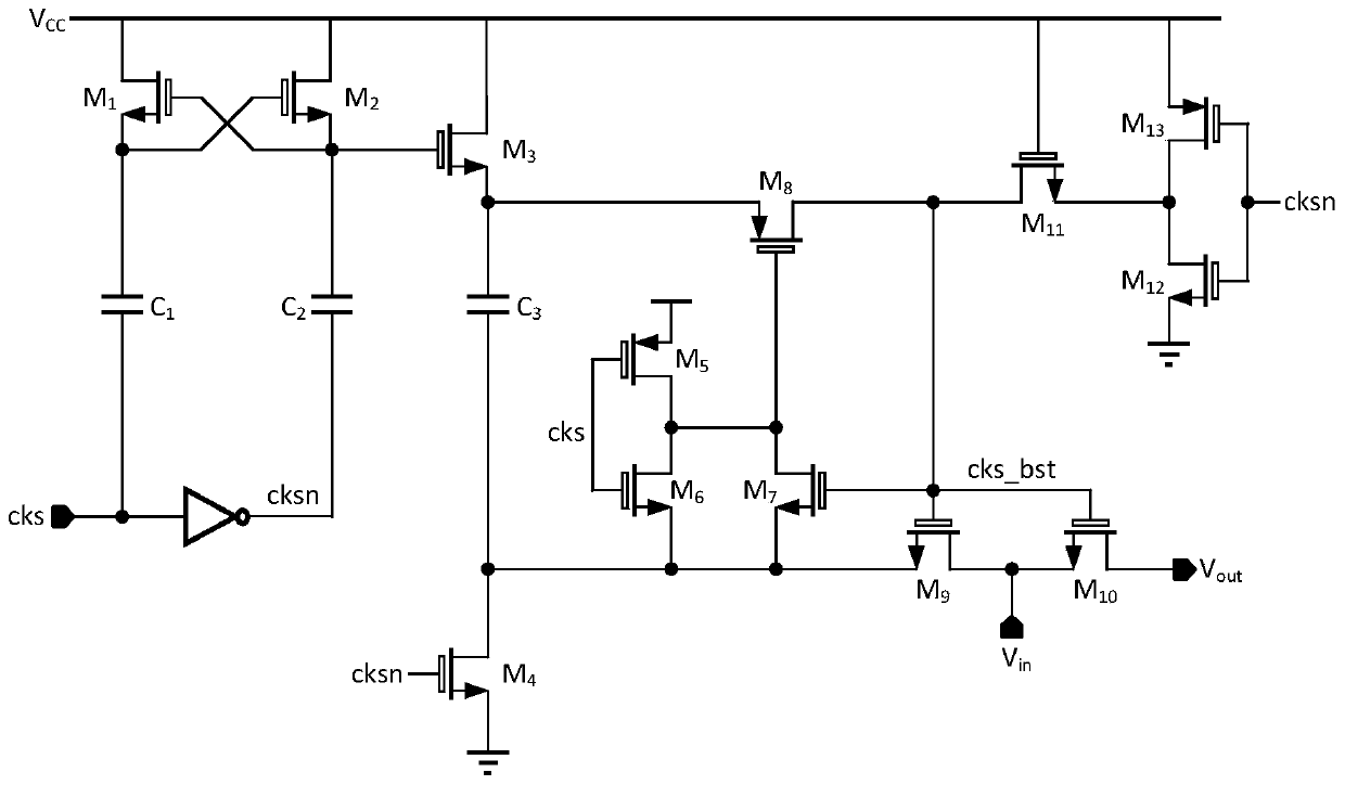
[0041] Figure 4 A bootstrap sampling switch circuit of this embodiment is shown. The bootstrap switch circuit includes: a voltage regulator 11 , a level shift circuit 12 and a bootstrap main circuit 13 .

[0042] The voltage regulator 11 is used to generate a first voltage Vdd_1p4 and a second voltage Vss_Op4, the first voltage Vdd_1p4 is equal to the common mode voltage VCM plus a third voltage, and the second voltage Vss_Op4 is equal to the common mode voltage VCM minus the third voltage , the third voltage is equal to half of the withstand voltage value of the low-voltage thin grid tube.

[0043] The level shift circuit 12 uses the first voltage Vdd_1p4 as a power supply voltage to generate a clock cks, the high level of the clock cks is equal to the first voltage Vdd_1p4, and the low level of the clock cks is equal to the the second voltage Vss_Op4.

[0044] The bootstrap main circuit 13 uses the first voltage Vdd_1p4 as the power supply voltage and the second voltage ...

Embodiment 2

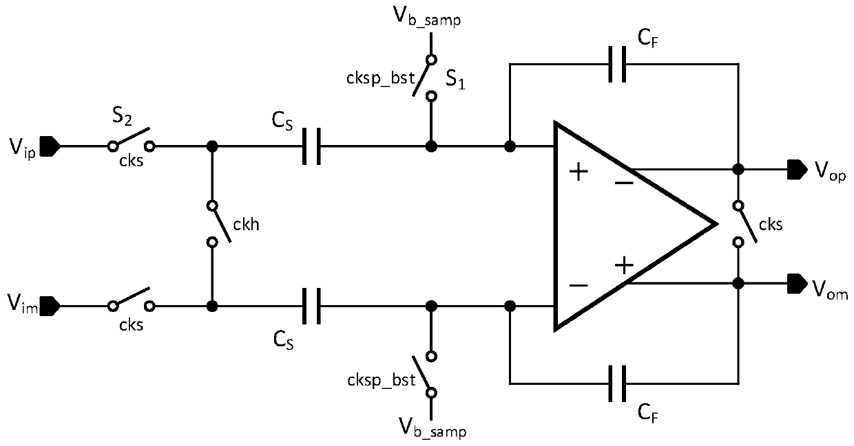
[0066] This embodiment provides a sample-and-hold circuit for an analog-to-digital converter. The sample-and-hold circuit includes a switch tube and the bootstrap sampling switch circuit in Embodiment 1. The clock cks generated by the bootstrap sampling switch circuit is used for control the switching tube. For example, the sample-and-hold circuit can use figure 1 In the circuit in the sampling process, the clock cks generated by the bootstrap sampling switching circuit controls the switch S2, and the switch S2 is realized by the switching tube Ms.

Embodiment 3

[0068] This embodiment provides an analog-to-digital converter, and the analog-to-digital converter includes the sample-and-hold circuit in Embodiment 2. Of course, in addition to the sample-and-hold circuit, the analog-to-digital converter may also include related circuits in other existing analog-to-digital converters.


PUM


Abstract

The invention discloses a bootstrap sampling switch circuit, a sampling hold circuit and an analog-to-digital converter. The bootstrap switching circuit comprises: a voltage regulator used for generating a first voltage and a second voltage, wherein the first voltage is equal to the sum of a common-mode voltage and a third voltage, and the second voltage is equal to the sum of the common-mode voltage and the third voltage; a level shift circuit, wherein the level shift circuit takes a first voltage as a power supply voltage and is used for generating a clock, the high level of the clock is equal to the first voltage, and the low level of the clock is equal to the second voltage; and a bootstrap main circuit, wherein the bootstrap main circuit takes a first voltage as a power supply voltageand takes a second voltage as ground, and the bootstrap main circuit is controlled by the clock and is used for generating a constant voltage at a gate-source end of the switching tube. The MOS tubesin the circuit are low-voltage thin gate tubes. The bootstrap sampling switching circuit is realized by adopting the low-voltage thin gate tube, so that the ascending and descending time of an outputclock is greatly shortened on the premise of not sacrificing the swing amplitude of an input signal, and the ADC sampling rate is greatly improved.

Description

technical field [0001] The invention belongs to the field of integrated circuits, in particular to a bootstrap sampling switch circuit, a sample hold circuit and an analog-to-digital converter. Background technique [0002] Analog-to-digital converters (ADC) are used to convert analog signals into digital signals, and are widely used in various data acquisition and communication systems. The sampling rate of the ADC directly determines the signal bandwidth that can be processed, and the accuracy of the ADC (such as the signal-to-noise ratio SNR, spurious-free dynamic range SFDR, etc.) determines the dynamic range of the entire system. ADC has a variety of architectures, such as pipelined ADC, successive approximation (SAR ADC), flash (flash ADC), time domain interleaved (interleavedADC) and so on. [0003] The working process of the ADC can be roughly divided into two processes: sampling and quantization. Sampling is to discretize the input signal at equal time intervals, ...

Claims


Application Information

Patent Timeline
IPC IPC(8): H03M1/12H03M1/46
CPCH03M1/1245H03M1/466
Inventor 张辉高远王海军李琪林李丹
Owner SHANGHAI BEILING
Why Eureka
Try Eureka