
Fin-like spacer-modulated hemt device based on transconductance compensation method and preparation method thereof

A compensation method and device technology, used in semiconductor/solid-state device manufacturing, semiconductor devices, electrical components, etc., can solve problems such as unsuitable high-frequency devices, large gate parasitic capacitance, and deterioration of device frequency characteristics.

Active Publication Date: 2021-09-14
XIDIAN UNIV
View PDF4 Cites 0 Cited by
  • Summary
  • Abstract
  • Description
  • Claims
  • Application Information

AI Technical Summary

Problems solved by technology

However, due to the large gate parasitic capacitance introduced by the insulating layer under the gate, the frequency characteristics of the device are deteriorated, and it is not suitable for making high-frequency devices.
[0010] In summary, the methods for improving device linearity in the prior art have the problems of large device etching damage, thick barrier layer, and large gate parasitic capacitance, which limits the application of linear devices at high frequencies.

Method used


Image

  • Fin-like spacer-modulated hemt device based on transconductance compensation method and preparation method thereof
  • Fin-like spacer-modulated hemt device based on transconductance compensation method and preparation method thereof
  • Fin-like spacer-modulated hemt device based on transconductance compensation method and preparation method thereof

Examples


Embodiment 1

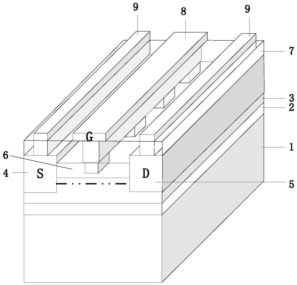
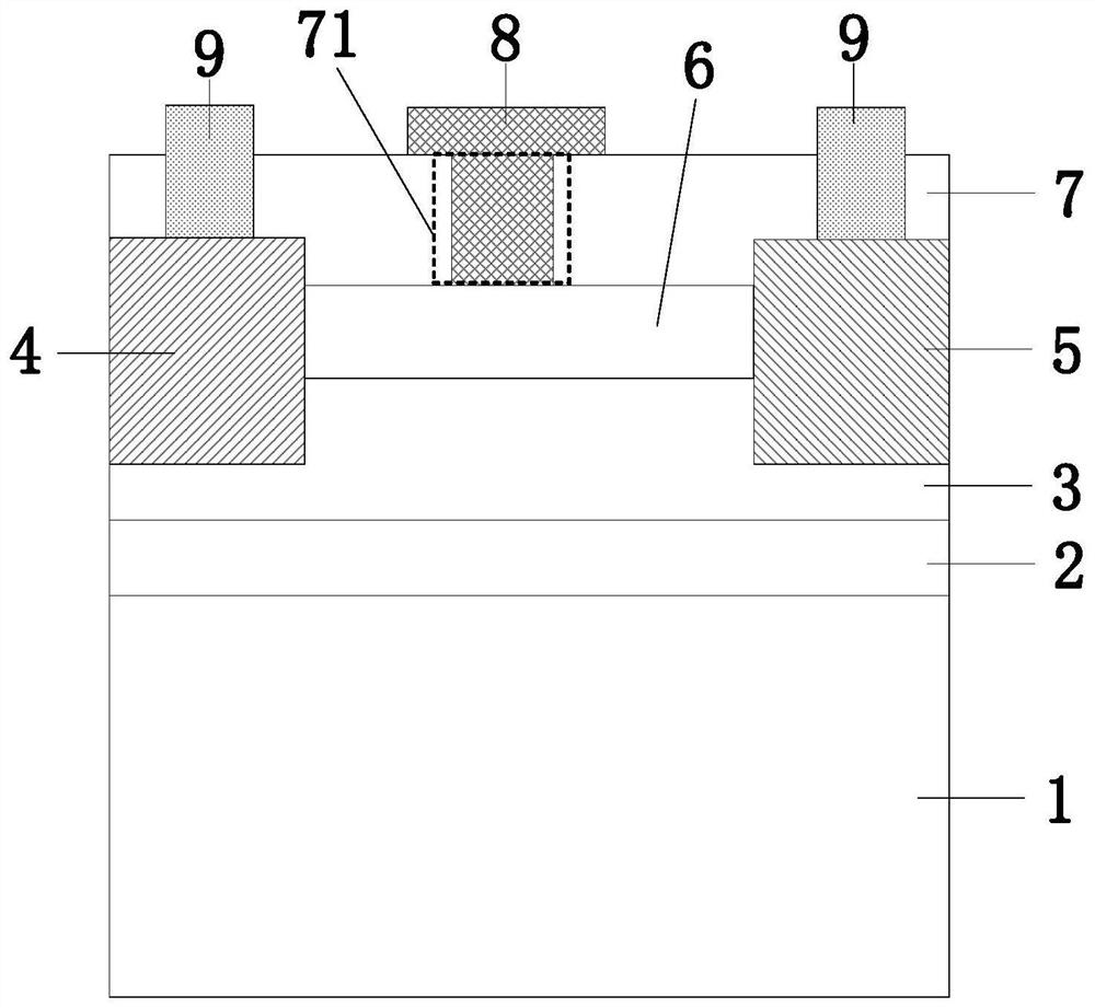
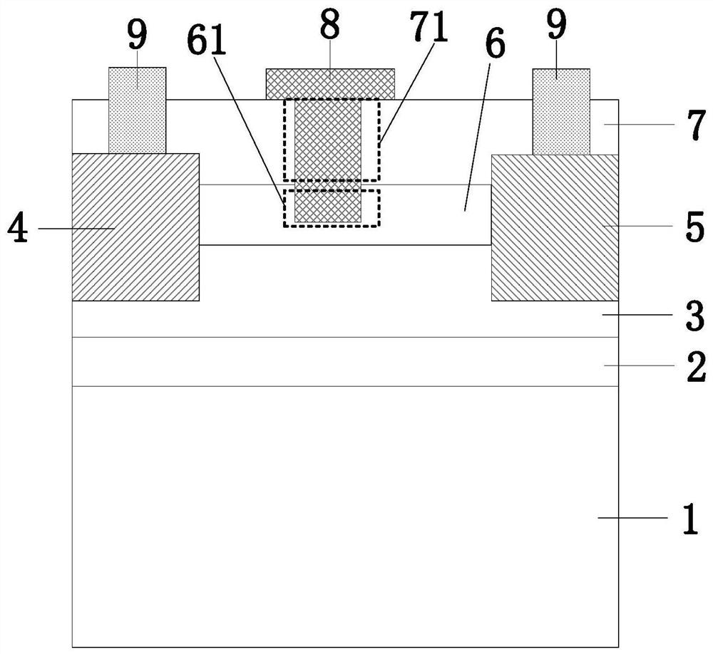
[0055] See figure 1 , figure 1 A schematic structural diagram of a Fin-like spacer modulation HEMT device based on a transconductance compensation method provided by an embodiment of the present invention, the HEMT device includes: a substrate layer 1, an insertion layer 2, a buffer layer 3, a source electrode 4, and a drain electrode 5. Barrier layer 6, passivation layer 7, gate electrode 8 and metal interconnection layer 9.

[0056] Specifically, the substrate layer 1 includes one or more of sapphire, SiC or Si. The insertion layer 2 is located on the substrate layer 1, and its material may be AlN. The buffer layer 3 is located on the insertion layer 2, and its material may be GaN. The source electrode 4 is located at one end of the buffer layer 3, and the drain electrode 5 is located at the other end of the buffer layer 3; the material of the source electrode 4 and the drain electrode 5 is ohmic metal, which is Ti / Al / Ni / Au from bottom to top. The barrier layer 6 is loca...

Embodiment 2

[0083] On the basis of Example 1, please refer to Figure 5 and Figure 6a-Figure 6h , Figure 5 A schematic flow chart of a method for manufacturing a Fin-like spacer-modulated HEMT device based on a transconductance compensation method provided by an embodiment of the present invention, Figure 6a-Figure 6h It is a schematic diagram of a method for manufacturing a Fin-like spacer-modulated HEMT device based on a transconductance compensation method provided by an embodiment of the present invention. The preparation method comprises steps:

[0084] S1 , growing an insertion layer 2 , a buffer layer 3 and a barrier layer 6 sequentially on the substrate layer 1 . See Figure 6a .

[0085] In this embodiment, an epitaxial substrate comprising a substrate layer 1, an AlN insertion layer 2, a GaN buffer layer 3, and an AlGaN barrier layer 6 from bottom to top is used as the initial material.

[0086] S2, prepare the source electrode 4 at one end on the buffer layer 3, and p...

Embodiment 3

[0160] On the basis of Embodiment 1 and Embodiment 2, please refer to Figure 7 , Figure 7 It is a schematic flowchart of another fabrication method of a Fin-like spacer-modulated HEMT device based on a transconductance compensation method provided by an embodiment of the present invention. The preparation method comprises steps:

[0161] S1 , growing an insertion layer 2 , a buffer layer 3 and a barrier layer 6 sequentially on the substrate layer 1 .

[0162] S2 , prepare the source electrode 4 at one end on the buffer layer 3 , and prepare the drain electrode 5 at the other end on the buffer layer 3 .

[0163] S3, photoetching the electrical isolation region of the active region on the AlGaN barrier layer 3, and manufacturing the electrical isolation of the active region of the device by using an ICP process.

[0164] S4 , growing a passivation layer 7 on the barrier layer 6 , the source electrode 4 and the drain electrode 5 in the active region.

[0165] S5 , etching t...


PUM

PropertyMeasurementUnit
thicknessaaaaaaaaaa
thicknessaaaaaaaaaa
thicknessaaaaaaaaaa

Abstract

The invention relates to a Fin-like sidewall modulated HEMT device based on a transconductance compensation method and a preparation method thereof. The HEMT device comprises: a substrate layer; an insertion layer located on the substrate layer; a buffer layer located on the insertion layer; a source electrode , located at one end of the buffer layer; the drain electrode, located at the other end of the buffer layer; the barrier layer, located on the buffer layer, and located between the source electrode and the drain electrode, wherein the barrier layer is provided with barriers arranged along the gate width direction Several grooves, the depth of the grooves is less than the thickness of the barrier layer; the passivation layer covers the source electrode, the drain electrode and the barrier layer, wherein, along the gate width direction, there are gate grooves running through the passivation layer, and A plurality of grooves are located under the gate groove; a gate electrode is located in the plurality of grooves and the gate groove, and is located on the surface of the passivation layer; a metal interconnection layer runs through the passivation layer and is located on the source electrode and the drain electrode. The HEMT device forms a Fin-like structure by arranging several grooves along the gate width direction, which can meet the application requirements of high frequency and high linearity and high voltage and high linearity.

Description

technical field [0001] The invention belongs to the technical field of semiconductor devices, and in particular relates to a Fin-like sidewall modulated HEMT device based on a transconductance compensation method and a preparation method thereof. Background technique [0002] In recent years, with the surge in demand for the Internet of Things and the development of mobile devices, people have higher requirements for the transmission efficiency of wireless communication technologies. For example, in millimeter wave applications such as 5G-LTE, WIMAX, satellite communication, radar, and space applications, the power amplifier (PA) is an important part of the communication link transmitter. In order to obtain sufficient transmission power, it must Work under the condition of high power output, but at this time PA will consume a lot of power, the linearity is very poor, resulting in low transmission efficiency, signal distortion and degradation of transmission quality, so in or...

Claims


Application Information

Patent Timeline
Patent Type & Authority Patents(China)
IPC IPC(8): H01L29/778H01L21/335H01L29/06
CPCH01L29/0684H01L29/66431H01L29/778
Inventor 宓珉瀚马晓华王鹏飞张濛郝跃
Owner XIDIAN UNIV
Learn More