Wafer cleaning equipment

A technology for cleaning equipment and wafers, applied to conveyor objects, discharge tubes, electrical components, etc., can solve problems such as increased equipment maintenance time and cost, pipeline leakage, and high sealing requirements for water and gas pipelines. Conducive to automation, simple heating operation, and guaranteeing the effect of production rhythm

Active Publication Date: 2020-07-28
北京晶亦精微科技股份有限公司
View PDF8 Cites 5 Cited by
  • Summary
  • Abstract
  • Description
  • Claims
  • Application Information

AI Technical Summary

Problems solved by technology

[0004] However, due to the solution cleaning method used in the existing equipment, there are a large number of pipelines and joints in the equipment, which require

Method used


Image

  • Wafer cleaning equipment
  • Wafer cleaning equipment
  • Wafer cleaning equipment

Examples


Embodiment Construction

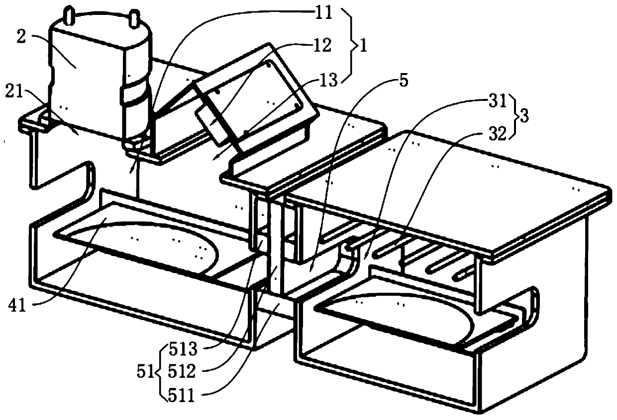
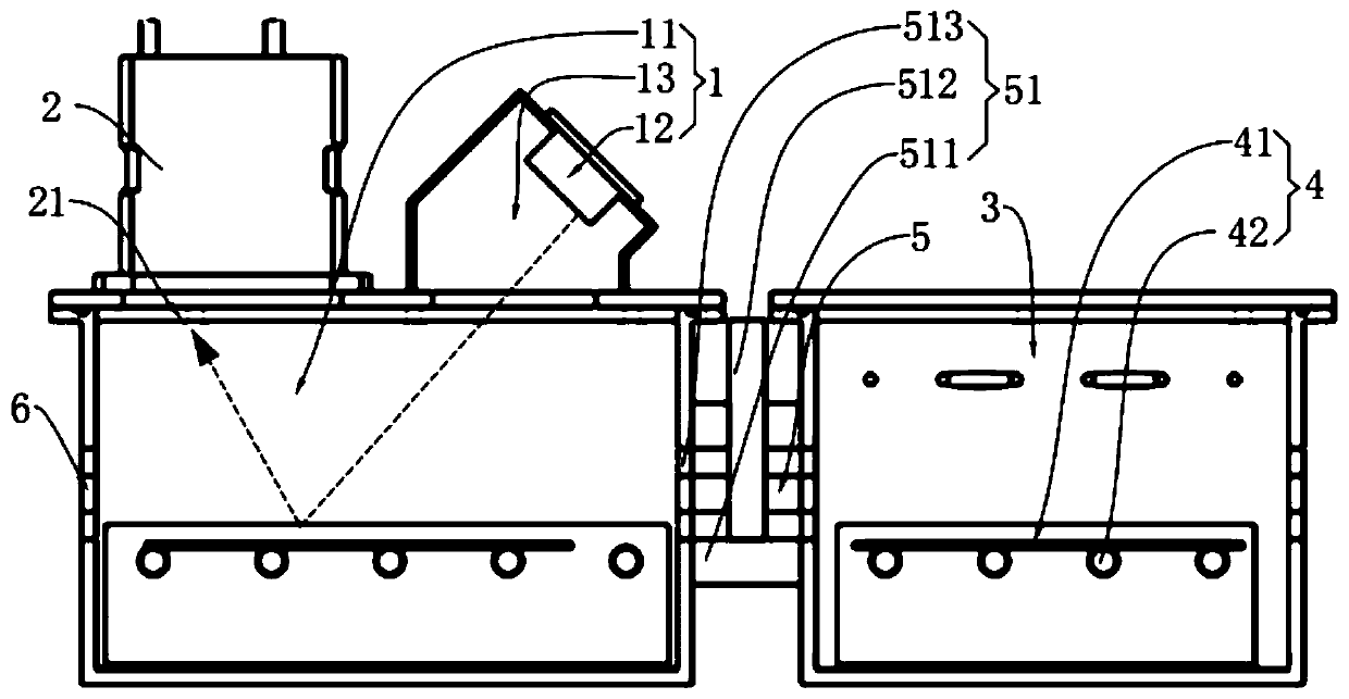
[0033] The technical solutions of the present invention will be clearly and completely described below in conjunction with the accompanying drawings. Obviously, the described embodiments are part of the embodiments of the present invention, rather than all of them. Based on the embodiments of the present invention, all other embodiments obtained by those of ordinary skill in the art without creative work shall fall within the protection scope of the present invention.

[0034] In the description of the present invention, it should be noted that the terms "center", "upper", "lower", "left", "right", "vertical", "horizontal", "inner", "outer", etc. The indicated orientation or positional relationship is based on the orientation or positional relationship shown in the drawings, and is only for the convenience of describing the present invention and simplifying the description, rather than indicating or implying that the pointed device or element must have a specific orientation or a ...


PUM


Abstract

The invention relates to the technical field of wafer cleaning. The invention relates to wafer cleaning equipment. The wafer cleaning equipment comprises a plasma cleaning assembly for removing residues on the surface of a wafer, the plasma cleaning assembly comprises a cleaning chamber and a plasma source, the cleaning chamber is used for placing a wafer, and the plasma source is located in the cleaning chamber and generates plasma beams to clean the wafer. The top end of the cleaning chamber is provided with an installation chamber, the plasma source is located in the installation chamber, the movement direction of a plasma beam generated by the plasma source is obliquely arranged relative to the wafer, and one side of the cleaning chamber is provided with an air extracting piece for extracting the cleaning chamber to be vacuum. The wafer is cleaned by plasma, a large number of pipelines and joints do not need to be installed in the equipment, and the later maintenance time and costof the equipment are reduced. Plasma is used for bombarding and cleaning the surface of the wafer, a rolling brush is prevented from being used and directly contacted with the surface of the wafer forremoving, and green damage-free cleaning is achieved. And as the plasma volume is smaller than that of water molecules, the plasma can go deep into micro holes of the wafer, and ion bombardment cleaning within a certain thickness on the surface of the wafer can be carried out.

Description

Technical field [0001] The invention relates to the technical field of wafer cleaning, in particular to a wafer cleaning equipment. Background technique [0002] The integrated circuit manufacturing process usually refers to depositing conductors, semiconductors, and insulating layers on a specific substrate (such as a silicon-based wafer) in a certain process sequence. In the manufacturing process, CMP (Chemical Mechanical Polishing) equipment is mainly used to planarize the surface of the wafer after the film is deposited for subsequent semiconductor processing. Since a certain amount of chemical liquid needs to be added for auxiliary polishing during the polishing process, the chemical liquid will remain on the surface of the wafer, so it needs to be cleaned after the polishing is completed to remove the residue on the surface of the wafer. [0003] In the invention patent with application publication number CN105789096A, a wafer cleaning equipment is disclosed, such as figure ...

Claims


Application Information

Patent Timeline
IPC IPC(8): H01L21/02H01L21/687H01L21/677H01L21/67H01J37/32
CPCH01L21/02065H01L21/02074H01L21/68785H01L21/67739H01L21/67017H01J37/32H01J2237/335Y02P70/50
Inventor 江伟尹影庞浩徐俊成
Owner 北京晶亦精微科技股份有限公司
Why Eureka
Try Eureka