A phase change material nanowire assembly, testing device and method
A test method, nanowire technology, applied in measurement devices, material resistance, nanotechnology, etc., can solve problems such as low success rate, disorderly arrangement of nanowires, instability, etc.
- Summary
- Abstract
- Description
- Claims
- Application Information
AI Technical Summary
Problems solved by technology
Method used
Image
Examples
Embodiment approach
[0044] According to an embodiment, the frequency of the applied electric field may be 1000KHz-10MHz, preferably, the frequency of the applied electric field is 500KHz-5000KHz, most preferably 100KHz-5000KHz.
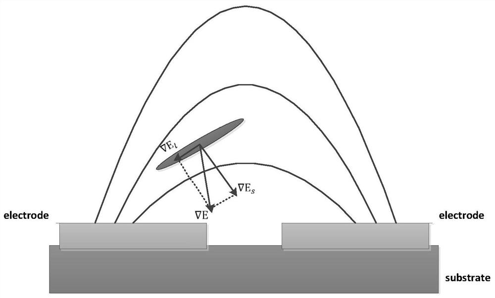
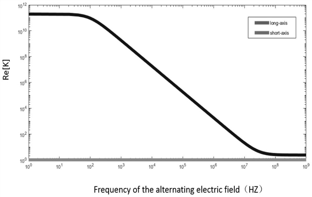
[0045] In the present invention, the theoretical analysis corresponding to the above-mentioned embodiment is as follows: In order to guide the orientation of the bismuth telluride nanowires to be accurately mounted on both ends of the comb electrode, the force analysis model of the bismuth telluride nanowires is constructed above, and Re[K l ] and Re[K s ] to represent the influence of the C-M factor on the axial and radial force of bismuth telluride nanowires, as follows:
[0046] The C-M factor of the simulated bismuth telluride nanowires along the axial long axis is expressed as:
[0047]
[0048] The C-M factor of the simulated bismuth telluride nanowires along the radial minor axis is expressed as:
[0049]
[0050] in,
[0051]
[0052] ω is the angular...
Embodiment 1
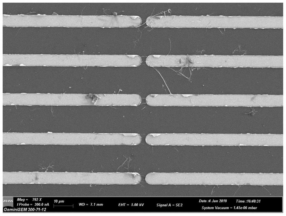
[0068] This embodiment provides a bismuth telluride nanowire electrical testing and assembly method, in which the bismuth telluride nanowire is overlapped between the pair of comb-shaped electrodes, and the specific steps are as follows:
[0069] Step 1: Provide platinum-titanium comb-shaped electrode pairs (which are formed by plating a metal film with an electron beam evaporation process and then etched using a photolithography process), in which there are 10 pairs of comb-shaped electrode pairs. The gap is 3um, and the distance between electrode pairs is 25um;
[0070] Step 2: placing the bismuth telluride nanowires prepared by the electrochemical method and the comb-shaped electrode of step 1 in the dielectric solution of ethanol to form a dielectrophoresis device;
[0071] Step 3: Apply an external electric field to the dielectrophoretic device in step 2, wherein the parameters of the external electric field are: electric field frequency = 500KHz, AC voltage = 1V, and rea...
Embodiment 2~14
[0075] Using the same method as in Example 1, selecting different external electric field parameters and comb electrodes, bismuth telluride assembled nano-components with different effects can be obtained. The conditions of the electrodes used and the parameters of the applied electric field are summarized in Table 1. According to the method in Example 1, the orientation connection amount of the bismuth telluride assembled nano-components prepared in each embodiment is measured, and the results are shown in Table 2. The calculation results of the effective probability and invalid probability of the orientation connection in Examples 1, 6 and 7 are shown in Table 3. .
PUM
| Property | Measurement | Unit |
|---|---|---|
| thickness | aaaaa | aaaaa |
| thickness | aaaaa | aaaaa |
Abstract
Description
Claims
Application Information


