High-speed high-efficiency high-voltage half-bridge gate drive circuit
A gate drive circuit and output drive circuit technology, which is applied in the field of high-speed, high-efficiency, high-voltage half-bridge gate drive circuits, can solve the problems of reducing the switching frequency of the system, increasing the damage of the switch, and increasing the driving delay.
Active Publication Date: 2020-08-04
HUANGSHAN UNIV +1
4 Cites 8 Cited by
AI-Extracted Technical Summary
Problems solved by technology
A relatively large series connection protection resistor will bring two problems. One is that the switch on the resistor is damaged and the ef...
Method used
Embodiment of the present invention, under fixed driving current condition, the work that Vout voltage and n reference voltages Vr1~Vrn carry out comparative quantification during 1us is realized by high-speed comparator array, and the function of this comparator array is similar to an ADC circuit, so there are many combinations of comparator arrays depending on the speed of load detection and quantization. N comparators can be used to compare and quantize the Vout voltage with n reference voltages Vr1~Vrn, and after a comparison of one clock cycle, the load quantization code Dout can be obtained. This overall scheme has the advantage of fast speed, but the comparator used The number is relatively large, and the hardw...
Abstract
The invention belongs to the technical field of integrated circuits. The invention particularly relates to a high-speed high-efficiency high-voltage half-bridge gate drive circuit used for driving a gate of a power device in a power electronic system. The circuit comprises an input receiving circuit, a dead zone signal generating circuit, a low-voltage generating circuit, a low-side signal delay circuit, a low-side high-efficiency output driving circuit, a low-delay high-voltage level shifting circuit and a high-side high-efficiency output driving circuit. According to the high-speed high-efficiency high-voltage half-bridge gate drive circuit provided by the invention, the delay of a level shift circuit is reduced through a positive feedback drive current enhancement technology such that the overall drive circuit speed is improved; the driving current can be adaptively adjusted according to the size of the load and the frequency of the input control pulse such that the power supply efficiency of the driving circuit is improved to the greatest extent; the gate drive circuit can be widely applied to various high-power-density power electronic systems, in particular to the gate driveapplication of wide bandgap power devices with higher frequency requirements.
Application Domain
Power conversion systems
Technology Topic
Integrated circuitLevel shifting +12
Image
Examples
- Experimental program(1)
Example Embodiment
[0049] The present invention will be described in further detail below with reference to the accompanying drawings and examples.
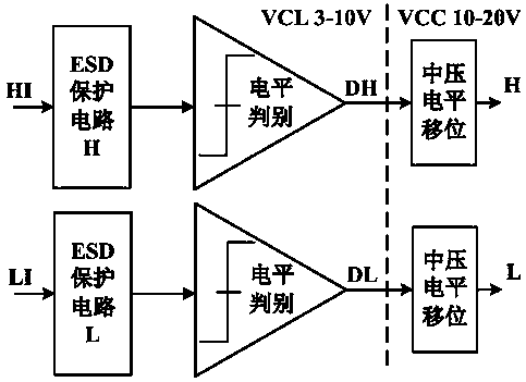
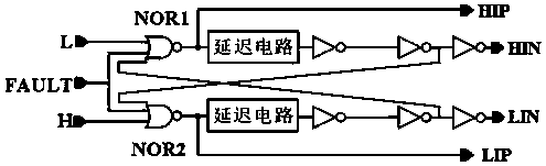
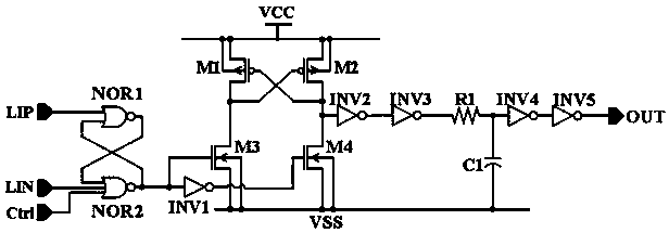
[0050] figure 1 It is a structural block diagram of the high-speed and high-efficiency high-voltage half-bridge gate drive circuit of the present invention. The high-speed and high-efficiency high-voltage half-bridge gate drive circuit includes an input receiving circuit, a dead-time generating circuit, a low-voltage generating circuit, a low-side delay circuit, a low-side high-efficiency output drive circuit L, and a low-latency high-voltage level shift circuit. and high-side high-efficiency output driver circuit H.
[0051] Among them, the low-voltage digital input signals HI and HI first enter the input receiving circuit, perform signal level discrimination and logic level high-voltage conversion, and obtain medium-voltage signals H and L; the dead-time generation circuit obtains the high-side differential input according to the medium-voltage signal H. The data HIP and HIN, according to the medium voltage signal L, obtain the low-side differential input data LIP and LIN; the high-side differential input data HIP and HIN enter the low-latency high-voltage level shift circuit to obtain the low-potential floating high-side driving data Din, Din enters the high-efficiency output drive circuit, and is amplified by the drive to obtain a high-side output signal HO with greater drive capability; the low-side differential input data LIP and LIN enter the low-side delay circuit to obtain low-side drive data, and output to the low-side high-side Efficiency output drive circuit L, which is driven and amplified to obtain a low-side output signal LO with greater drive capability;
[0052] The low-side high-efficiency output drive circuit L and the high-side high-efficiency output drive circuit H are high-efficiency output drive circuits with the same circuit structure; the low-latency high-voltage level shift circuit needs to use low-voltage ground VSS and The floating ground SW has two sets of ground potentials. The high-side high-efficiency output drive circuit H only needs to use the floating ground SW, the input receiving circuit, the dead-time generating circuit, the low-voltage generating circuit, the low-side delay circuit and the low-side high-efficiency output. The driving circuit L uses the low-voltage ground VSS in common; the driving capability of the high-efficiency output driving circuit is controlled by the power-on signal Start-up, Clk-ctrl of the trigger control clock signal and n reference voltages Vr1-Vrn; the input receiving circuit needs The low-voltage power supply voltage VCL and the medium-voltage power supply voltage VCC are used simultaneously; the low-voltage generating circuit generates the low-voltage power supply voltage VCL and n reference voltages Vr1-Vrn according to the medium-voltage power supply voltage VCC; wherein, n is any positive integer.
[0053] A basic input receiving circuit structure that can be used for the high-voltage gate driver chip of the present invention is as follows: figure 2 As shown, including the same two input channels, each channel contains input ESD protection, level decision circuit and medium voltage level shift circuit. The input receiving circuit not only needs to complete the transmission of the signal, but also complete the ESD protection of the circuit inside the chip, so as to prevent the circuit from being damaged due to the impact on the inside of the circuit caused by ESD. The ESD protection circuits commonly used in integrated circuit design include: lateral SCR clamp circuit, anti-parallel diode clamp circuit, Zener clamp circuit and CDM clamp, etc. The level judgment circuit is used to identify whether the external input level is a logic "0" or "1". Due to the large interference of external signals, the level judgment circuit must have sufficient anti-interference noise tolerance. The specific circuit implementation usually includes two types. In the form of a Schmitt trigger and a hysteresis comparator. Depending on the speed at which the driver chip drives the object and the input logic signal, the implementation circuits of Schmitt triggers and hysteresis comparators are very different. Since the power supply voltage VCC of the gate driver chip is usually a medium voltage level of 10~20V, and the input logic level is an external digital logic lower than 5V, in order to complete the judgment of the input logic level more accurately, input ESD and power The flat-decision circuit must use a relatively lower supply voltage VCL, usually 3-10V. Therefore, before the logic signal output by the level decision circuit enters the internal control logic of the chip, it must go through a medium voltage level shift circuit to convert the logic signal whose high level is VCL into a logic signal whose high level is VCC, and obtain H and L Signal.
[0054] Due to the large gate parasitic capacitance of the power device, when the device is turned on or off, it takes a certain amount of time to charge and discharge the capacitor, and it is necessary to prevent the direct connection between the two power devices of the upper and lower bridge arms being driven. Setting the dead time is a control method to ensure the reliable operation of the high- and low-side power devices. Make sure that one device is completely off before turning the other on. The dead time generation circuit is to add the input square wave to the dead time as the driving signal of the high and low side gates. The basic structure block diagram of the dead time generating circuit of the present invention is as follows image 3 shown. The dead zone is generated by the circuit by using a delay circuit to generate a phase difference between the two input signals, and then performing logical operations on the input signal to obtain a dead zone time. The size of the dead time is determined by the delay time generated by the delay circuit, so the delay circuit is the core of the dead time circuit. The simplest structure of the delay circuit is an inverter + RC network, but this method is not accurate enough and can only meet the needs of medium and low speed applications. The realization of the delay circuit with higher precision can be through the structure of the capacitance, the structure of the current source and the structure of resistance.
[0055]After the high-end signal passes through the level shift circuit, a certain delay is generated compared to the low-end signal. For the application of medium and high frequency, the phase mismatch of high and low-end signals has been caused during this period, which will affect the normal operation of the system. Therefore, a delay matching circuit must be added to the low-end signal path to achieve phase matching of the high- and low-end signals. The structure of the low-side delay circuit according to the present invention is as follows Figure 4 shown. From a structural point of view, the delay circuit first converts the signal by the RS flip-flop, and then uses a cross-coupling circuit to make the rising and falling edges of the signal steeper, and then passes through the RC network to delay the signal.
[0056] The low-voltage power supply circuit is a basic functional module that any analog IC must be equipped with. The implementation structure block diagram that can be used by the high-voltage half-bridge gate drive circuit of the present invention is as follows: Figure 5 shown. The bias and power supply circuit includes a start-up circuit, a bandgap reference circuit and a buffer, a bias circuit and an input low voltage generating circuit. After the chip's VCC voltage is powered on, the startup circuit is the first circuit in the entire chip. The startup circuit usually provides a certain initial bias signal to the bandgap reference voltage generation circuit to generate a fixed reference voltage and reference current; the reference voltage then passes through The reference voltage generation circuit is used to generate various reference voltages Vr1, Vr2~Vrn required for the internal operation of the chip, and output through the drive buffer circuit; the reference current usually enters the bias signal generation circuit to generate various bias signals for the internal operation of the chip. Other analog circuits provide bias, and also provide bias for the reference voltage generation circuit and the input interface module low-voltage power supply circuit; the input low-voltage generation circuit usually generates a 3-10V floating low-voltage power supply voltage VCL.
[0057] Image 6 It is the structure diagram of the low-latency high-voltage level shift circuit of the present invention, which is in the figure 2 On the basis of this, the simple RS flip-flop is improved into a highly reliable error hysteresis filter circuit, and the enhancement transistors Me1 and Me2 that accelerate the rising speed of LSP and LSN are added, and the signal inversion detection circuit that controls Me1 and Me2 is added. The low-latency high-voltage level shift circuit includes: a first high-voltage LDMOS transistor MD1, a second high-voltage LDMOS transistor MD2, a first protection diode D1, a second protection diode D2, a third resistor R3, and a fourth resistor R4, first resistor R1, second resistor R2, first coupled MOS transistor M1, second coupled MOS transistor M2, first speed enhancement transistor Me1, second speed enhancement transistor Me2, error hysteresis filter circuit and signal inversion detection circuit.
[0058] The source terminals of the first high-voltage LDMOS transistor MD1 and the second high-voltage LDMOS transistor MD2 are connected to the low-voltage ground VSS; the drain terminal of the first high-voltage LDMOS transistor MD1 is simultaneously connected to the source terminal of the first coupling MOS transistor M1 and the first protection diode D1. The anode, the lower end of the third resistor R3 and the gate end of the second coupling MOS transistor M2; the drain end of the second high voltage LDMOS transistor MD2 is simultaneously connected to the source end of the second coupling MOS transistor M2, the anode of the second protection diode D2, The lower end of the fourth resistor R4 and the gate end of the first coupling MOS tube M1; the drain end of the first coupling MOS tube M1 is connected to the upper end of the first resistor R1, and is also connected to the data input P end LSP and the first end of the error hysteresis filter circuit. The drain terminal of a speed enhancement transistor Me1; the drain terminal of the second coupling MOS transistor M2 is connected to the upper end of the second resistor R2, and is also connected to the data input N terminal LSN of the error hysteresis filter circuit and the drain terminal of the second speed enhancement transistor Me2 The lower ends of the first resistor R1 and the second resistor R2 are connected to the floating ground SW; the output of the error hysteresis filter circuit is the drive data Din, and Din is also used as the input signal of the signal inversion detection circuit at the same time; the 2 output ends of the signal inversion detection circuit are respectively The gate terminals of the first speed enhancement transistor Me1 and the second speed enhancement transistor Me2 are connected; the cathode of the first protection diode D1, the cathode of the second protection diode D2, the upper end of the third resistor R3, the upper end of the fourth resistor R4, the first The source terminal of the speed enhancing transistor Me1 and the source terminal of the second speed enhancing transistor Me2 are simultaneously connected to the high voltage power supply voltage.
[0059] Figure 7 It is a schematic diagram of the principle of reducing the delay of the low-latency high-voltage level shift circuit of the present invention. Assuming that HIP inputs a pulse, after a certain time delay Din will change and start to rise from 0. For the conventional level shift circuit without delay optimization, the rise delay time of Din is td. The principle of delay optimization of the present invention is to detect the change of Din through the signal inversion detection circuit, and accelerate the inversion speed of Din when it exceeds a certain threshold. At time t0, LSP voltage starts to change from 0 low to high, causing Din to change from low to high from SW (VH voltage at this time); at time tdet, when the signal inversion detection circuit confirms that Din is changed from low to high and the Din voltage exceeds the signal inversion When the threshold value of the detection circuit is Vth-det, the signal inversion detection circuit turns on the second speed enhancement transistor Me2 to accelerate the voltage rise speed of LSP, thereby accelerating the voltage rise process of Din rising from Vth-det to the high voltage power supply VH+VCC; at tden time, Din can complete the flip from low to high potential. For example, if Vth-det is set at 20% of the VCC voltage, the overall transition time tden of Din from low to high can be reduced to 30% of the original td, that is, the signal transmission delay from HIP to Din is reduced to 30%, The corresponding driving circuit speed can be increased by more than 3 times. Obviously, setting Vth-det at different thresholds has a direct impact on the order of tden. The smaller the Vth-det, the smaller the tden and the shorter the delay, but it is more sensitive to the error fluctuation of LSP. Therefore, it is necessary to design high anti-interference. The performance error hysteresis filter circuit filters out various error disturbances on the LSP and LSN.
[0060] Figure 8 It is a structural diagram of a highly reliable error hysteresis filter circuit that can be used in the present invention. The circuit includes: P-terminal coupled inverter, P-terminal deglitch circuit, P-terminal OR gate, P-terminal data selector, N-terminal coupled inverter, N-terminal deglitch circuit, N-terminal OR gate and N-terminal data selection The P-terminal deburring circuit has the same structure as the N-terminal deburring circuit, and it contains three 2-input NAND gates and one 2-input OR gate.
[0061] for Image 6 The medium signal inversion detection circuit can be realized by a conventional combinational logic circuit. The simplest way is an inverter circuit, or an inverter circuit with a control function added. The inversion threshold of the inverter is Vth-det; the realization of higher precision The method can be realized by a high-speed comparator. One end of the comparator is Vth-det, and the other end is Din.
[0062] Figure 9 It is a structural block diagram of the high-efficiency output drive circuit of the present invention, including an input P-terminal inverter chain, an N-terminal inverter chain, n P-terminal output inverters, n N-terminal output inverters, and n P-terminal output inverters. PMOS transistors Mp1-Mpn, n N-terminal output NMOS transistors Mn1-Mnn, n P-terminal output inverter control switches, n N-terminal output inverter control switches, sampling switch SW, input data switch Kin and test data Switch Kcal, high-speed comparator array, error filter circuit, load discrimination circuit, drive current selection circuit, input pulse frequency discrimination circuit and controller circuit;
[0063] The P-side inverter chain includes k cascaded P-side input buffer inverters, and the driving capability of the k inverters gradually increases from the previous stage to the subsequent stage; the N-terminal inverter chain includes k -1 cascaded N-terminal input buffer inverter and a delay unit (delay), the driving capability of k-1 inverters gradually increases from the previous stage to the subsequent stage; the delay time of the delay unit (delay) must be equal to the delay time of the front-end P-terminal input buffer inverter; the output of the P-terminal inverter chain is connected to the left side of the n P-terminal output inverter control switches at the same time, and the N-terminal inverter The output of the chain is simultaneously connected to the left side of the n N-terminal output inverter control switches; the P-terminal inverter chain is connected to the input terminal of the N-terminal inverter chain, and is also connected to the input data switch Kin and test data The right side of the switch Kcal; the right sides of the n P-terminal output inverter control switches are respectively connected to the gate terminals of the n P-terminal output PMOS transistors, and the right sides of the n N-terminal output inverter control switches are respectively connected to n N N terminals. The gate terminals of the NMOS transistors are connected to the gate terminal of the NMOS transistors; the source terminals of the n P terminal output PMOS transistors are connected to the power supply voltage at the same time, the source terminals of the n N terminal output NMOS transistors are connected to the ground at the same time, and the drain terminals of the n P terminal output PMOS transistors are simultaneously connected to the ground. Connected to the drain terminals of n N-terminal output NMOS transistors and the output Vout of the high-efficiency output drive circuit;
[0064] The output Vout of the high-efficiency output drive circuit is sampled by the sampling switch SW, and then enters the high-speed comparator array, and is compared with n reference voltages to obtain the quantization code Dout and enter the error filtering circuit, and output the load detection code Dtest after filtering; the input pulse frequency is judged The circuit compares and quantifies the frequency of the input data Din based on the test clock Clkcal, and obtains the Din frequency discrimination code Dfin; the load detection code Dtest and the frequency discrimination code Dfin enter the load discrimination circuit at the same time to calculate the load evaluation code Dev; the drive current selection circuit is based on Dev. size, select and output n switch control signals Kp1~Kpn of the P-terminal output inverter control switch and n switch control signals Kn1~Knn of the N-terminal output inverter control switch;
[0065] The load test signal Dcal output by the controller circuit is connected to the left side of the test data switch Kcal, the test clock Clkcal output by the controller circuit is connected to the clock input terminal of the input pulse frequency discrimination circuit, and the load test control signal Ctrl_test output by the controller circuit is respectively It is connected to the control signal input end of the high-speed comparator array and the error filtering circuit, the control signal Ctrl_ev output by the controller circuit is connected to the control signal input end of the load discrimination circuit, and the Ctrl_out signal output by the controller circuit is connected to the control signal of the drive current selection circuit Signal input terminal, the Ctrl_fin signal output by the controller circuit is connected to the control signal input terminal of the input pulse frequency discrimination circuit; the controller circuit is controlled by the trigger control clock signal Clk-ctrl and the power-on signal Start-up; the trigger control clock signal The frequency of Clk-ctrl must be R times the frequency of the load test signal Dcal; wherein, n, k and R are all any positive integers.
[0066] Figure 9 The high-efficiency output driving circuit according to the present invention is shown, and its working state includes two modes of self-adaptive adjustment of driving capability and normal operation. After the power supply voltage is powered on, the high-efficiency output driving circuit first starts the driving capability self-adaptive adjustment mode, and then enters the normal working mode.
[0067] The adaptive adjustment process of the drive capability of the high-efficiency output drive circuit is as follows: Figure 10 shown. When the power supply voltage is powered on, the power-on Start-up signal becomes valid from low to high; the controller circuit will turn off the input data switch Kin, output the test clock Clkcal, and turn on the deep pulse frequency discrimination circuit. The input pulse frequency discrimination circuit is based on the test clock Clkcal compares and quantifies the frequency of the input data Din and obtains the Din frequency discrimination code Dfin; the controller circuit then turns on the test data switches Kcal, Kp1 and Kn1, and outputs the load test signal Dcal, and also turns on the high-speed comparator array and error filtering. circuit, load discrimination circuit and drive current selection circuit. At this time, the output Vout of the drive circuit will produce different dv/dt changes according to different loads; after the Dcal output, the Mth Clk-ctrl clock edge, when the output setup time ( After the time required for the Vout voltage to rise) is satisfied, the controller circuit will turn on the sampling switch SW to sample the Vout voltage, and process the high-speed comparator array and the error filtering circuit to obtain the load detection code Dtest; The Din frequency discrimination code Dfin is calculated to obtain the load evaluation code Dev; the drive current selection circuit sets the switch control signals Kp2 to Kpn and Kn2 to Knn according to the load evaluation code Dev, and keeps them unchanged; at this time, the high-efficiency output The output drive capability of the drive circuit remains unchanged, ending the drive capability adaptive adjustment mode; the controller circuit finally turns on the switch Kin, turns off the switch Kal and the load test signal Dcal, and the output drive circuit starts the normal operation mode.
[0068]The drive capability adaptive adjustment process of the output high-efficiency drive circuit is triggered by the power-on Start-up signal, the power-on Start-up signal becomes valid from low to high, and the control clock Clk-ctrl enters the controller circuit; the controller circuit will Output the test clock Clkcal, turn on the in-depth pulse frequency discrimination circuit, the input pulse frequency discrimination circuit compares and quantifies the frequency of the input data Din based on the test clock Clkcal, and obtains the Din frequency discrimination code Dfin after J test clocks Clkcal clocks; the controller circuit then outputs Load test signal Dcal. At this time, the output Vout of the drive circuit will produce different dv/dt changes according to different loads; at the Mth Clk-ctrl clock edge after the Dcal output, the controller circuit will turn on the sampling switch SW to measure the Vout voltage Sampling and processing by the high-speed comparator array and error filtering circuit to obtain the load detection code Dtest; the load judgment circuit calculates the load evaluation code Dev according to the load detection code Dtest and Din frequency judgment code Dfin on the Juge clock edge, and keeps it unchanged ;The drive current selection circuit sets the switch control signals Kp2~Kpn and Kn2~Knn according to the load evaluation code Dev, and keeps them unchanged; Finally, the power-on Start-up signal becomes invalid from high to low, and the output drive circuit outputs The drive capability remains unchanged, and the drive capability adaptive adjustment mode ends.
[0069] In the process of self-adaptive adjustment of the driving capability, the frequency of the control clock Clk-ctrl must be much higher than the frequency of the input data Din, for example, the frequency of Din is 100KHz, and the frequency of Clk-ctrl is usually set above 10MHz; the frequency of the test clock Clkcal cannot be low. In order to control the frequency of the clock Clk-ctrl, the higher the Clkcal frequency is, the more accurate the judgment of the Din frequency is.
[0070] In the process of comparing and quantizing the frequency of the input data Din by the input pulse frequency discriminating circuit, the time length of the J test clock cycles of Clkcal must be greater than the integer cycle of Din. For example, if the frequency of Din is 100KHz, and the frequency of the test clock Clkcal is 10MHz, the corresponding signal periods of Din and Clkcal are 10us and 0.1us respectively, then the value of J must be greater than 100. If the frequency of Clkcal is X times the frequency of Din, then J must be a positive integer greater than X. Obviously, the larger the value of J, the more accurate the value of Dfin, and X is a positive number greater than 1.
[0071] The time span of the Mth Clk-ctrl clock edge after the output of the Dcal must be less than one cycle time of the Dcal. For example, the frequency of Dcal is 200KHz and the frequency of Clk-ctrl is 5MHz, then the corresponding signal periods of Dcal and Clk-ctrl are 5us and 0.2us respectively, then the value of M must be less than 25. Obviously, the closer the value of M is to 25, the more accurate the value of Dtest is. .
[0072] Figure 11 It is an explanatory diagram of the load detection principle of the present invention. Assumption Figure 10 After the high-efficiency output driving circuit shown is turned on Kp1 and Kn1, the output current provided by the N-terminal NMOS transistor Mn1 and the P-terminal output PMOS transistor Mp1 is Iout=0.5A, and the frequency of Clk-ctrl is 5MHz (corresponding to the signal period of 0.2us ), select M=5, then the sampling switch SW will sample the Vout voltage when the high level of Dcal starts for 1us. For a fixed output Iout, it is obvious that the larger the driven load capacitance, the lower the rising slope of Vout, and the Vout voltage at 1us is inversely proportional to the load capacitance, that is, the Vout voltage when the load is 0.5nF should be when the load is 1.5nF. 3 times the Vout voltage. Therefore, under the condition of a fixed driving current, the size of the output driving load can be determined according to the size of the Vout voltage at 1us, and the size of the output driving load can be determined by comparing the Vout voltage with n reference voltages Vr1 ~ Vrn Perform quantization to obtain the load quantization code Dout.
[0073] In the embodiment of the present invention, under the condition of a fixed drive current, the work of comparing and quantifying the Vout voltage with n reference voltages Vr1 to Vrn at 1us is realized by a high-speed comparator array. The function of the comparator array is similar to that of an ADC circuit. Therefore, Depending on the quantization speed of load detection, there are many combinations of comparator arrays. N comparators can be used to compare and quantify the Vout voltage with n reference voltages Vr1~Vrn. After a clock cycle comparison, the load quantization code Dout can be obtained. The overall scheme has the advantage of high speed, but the comparators used The number is relatively large, and the hardware overhead is large; a comparator can also be used to compare and quantize the Vout voltage with the n reference voltages Vr1 ~ Vrn successively, so as to obtain the load quantization code Dout. The overall scheme has the advantage of small hardware overhead, but the same A comparator is used multiple times and is relatively slow. There are also settings of n reference voltages Vr1 to Vrn in combination with the comparator combination strategy, which can be set at uniform intervals by thermometer codes, or set with different binary weights. Therefore, in actual implementation, the appropriate comparator type and combination strategy can be selected according to the requirements of the driver chip application system.
[0074] Because the high-speed comparator has a certain offset, and the higher the operating speed of the comparator, the more serious the offset will be. Therefore, it is necessary to perform error filtering on the load quantization code Dout to obtain the load detection code Dtest. The implementation of the error filter circuit depends on the type of Dout code and the front end. Combination implementation strategies of high-speed comparator array circuits vary greatly. If the comparator array circuit uses n comparators to work in parallel, the digital algorithm for offset calibration of the Flash ADC comparator needs to be used for error filtering; if the comparator array circuit uses one comparator multiplexing, it needs to use SAR A digital algorithm for ADC offset calibration performs error filtering.
[0075] Figure 12 The block diagram of the load judging circuit of the present invention is shown, and the circuit includes 2 registers 1 and 2 for storing the load detection code Dtest and the frequency judgment code Dfin respectively, and the load detection code Dtest and the frequency judgment code Dfin. A normalized quantization calculation circuit for calculation processing. The data outputs of register 1 and register 2 are controlled by the Juge signal. The load evaluation code Dev output by the normalized quantization calculation circuit is calculated by Dtest and Dfin, and the calculation formula is: Dev=G*Dtest/Dfin. Among them, G is a gain coefficient, which is an empirical value, and is selected according to the application background of the output driving circuit of the present invention. In practical applications, G is usually a positive number greater than 1.
[0076] The actual function of the normalized quantization calculation circuit is to further optimize the output drive current of the output drive circuit of the present invention according to the frequency of the input data Din. Since the load test signal Dcal is a fixed frequency signal, after the output load is tested, if the frequency of the input data Din is much less than the frequency of Dcal, the driving current can continue to be reduced, thereby further improving the efficiency of the driving circuit and saving unnecessary power consumption overhead. For example, the corresponding signal periods of Din and Dcal are 10us and 1us respectively. Compared with a fixed load, the frequency of Din is 10 times slower, and the charging time for the load capacitor can be extended by 10 times, so a smaller drive current can be selected to charge the output load. discharge. Therefore, under the condition that the requirements of the driving circuit application system are met, the coefficient G can be set to scale the value of Dev to reduce the output driving current, further improve the efficiency of the driving circuit, and save unnecessary power consumption overhead.
[0077] Figure 13 This is a block diagram of the controller circuit of the present invention. The function of the controller circuit is to provide the control signals required for other circuits to work according to the external trigger control clock signal and the power-on signal. The controller circuit includes: a frequency discrimination control generation circuit for generating the Ctrl_fin signal to control the input pulse frequency discrimination circuit; a switch signal generation circuit for generating switch control signals Kcal, SW and Kin; a load test control generation circuit for for generating the load test control signal Ctrl_test to control the high-speed comparator array and the error filtering circuit; the load discrimination control generation circuit for generating the Ctrl_ev signal to control the load discrimination circuit; the drive current control generation circuit for generating the Ctrl_out signal to control the drive current selection circuit; The test code generation circuit is used to generate the load test code Dcal; the counter circuit is used to control the clock signal Clk-ctrl and the power-on signal Start-up according to the external trigger, and provide the other control signals according to the sequence to generate the required trigger signal.
[0078] The input pulse frequency judging circuit of the present invention has a circuit function of comparing and quantifying the frequency of the input data Din by using the test clock Clkcal, which can be realized by a phase detector circuit. The function of the drive current selection circuit can use a decoder or a multiplexer to realize signal switch selection.
[0079] The above are only preferred embodiments of the present invention and are not intended to limit the present invention. Any modifications, equivalent replacements, improvements, etc. made within the spirit and principles of the present invention shall be included in the protection of the present invention. within the range.
PUM


Description & Claims & Application Information
We can also present the details of the Description, Claims and Application information to help users get a comprehensive understanding of the technical details of the patent, such as background art, summary of invention, brief description of drawings, description of embodiments, and other original content. On the other hand, users can also determine the specific scope of protection of the technology through the list of claims; as well as understand the changes in the life cycle of the technology with the presentation of the patent timeline. Login to view more.