Integral bleeder circuit based on composite dielectric gate double-transistor photosensitive detector

A photosensitive detector and two-transistor technology, applied in circuits, electric solid-state devices, semiconductor devices, etc., can solve the problems of unfavorable chip miniaturization, large area, high power consumption, etc., so as to reduce the use of operational amplifiers and reduce power consumption. Effects with area, high power consumption

Pending Publication Date: 2020-08-14
NANJING UNIV
View PDF1 Cites 0 Cited by
  • Summary
  • Abstract
  • Description
  • Claims
  • Application Information

AI Technical Summary

Problems solved by technology

Most of the existing integral bleeder circuits are implemented by cascading multiple operational amplifiers,

Method used


Image

  • Integral bleeder circuit based on composite dielectric gate double-transistor photosensitive detector
  • Integral bleeder circuit based on composite dielectric gate double-transistor photosensitive detector
  • Integral bleeder circuit based on composite dielectric gate double-transistor photosensitive detector

Examples


Example Embodiment

[0025] Example 1

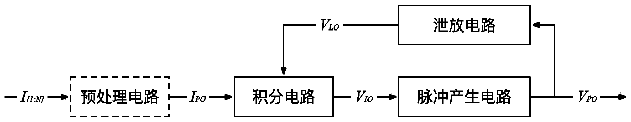
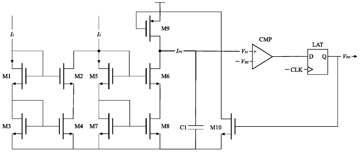
[0026] In this embodiment, an integral bleeder circuit based on the linear integral synchronous bleeder of the composite dielectric gate two-transistor photosensitive detector is introduced, such as image 3 shown. Among them, M1~M9 constitute a preprocessing circuit, and the preprocessing output signal I PO for preprocessing the input signal I 1 , I 2 Difference. Capacitor C1 constitutes an integral circuit to complete the linear integral operation. CMP and LAT form a pulse generation circuit, and complete the pulse generation output signal V PO production. M10 constitutes a discharge circuit to complete the charge discharge function of the integrating circuit. The specific circuit is as follows: Preprocessing the input signal I 1 It is connected with the drain terminal and gate terminal of the transistor M1 and the gate terminal of the transistor M2 to preprocess the input signal I 2It is connected to the drain terminal of transistor M2, the drain...

Example Embodiment

[0028] Example 2

[0029] In this embodiment, an integrating and bleeder circuit for the positive and negative arrays of the composite dielectric gate double transistor photodetector is introduced, such as Figure 4 shown. C1, C2 and M0 constitute a composite dielectric gate double-transistor photodetector. The gray part on the left is a 2×2 composite dielectric gate double-transistor photodetector array that represents a positive number to form a positive array, and the gray part on the right is 2×2. The composite dielectric gate two-transistor photodetector array representing negative numbers constitutes a negative array. The integral bleeder circuit adopts the circuit of Embodiment 1. The positive array and the negative array are connected with the source terminals of each column of composite dielectric gate double transistor photodetectors to form source lines (the other interfaces are not shown). Integral bleeder circuit #1 is used to calculate the first source line of...


PUM


Abstract

The invention discloses an integral bleeder circuit based on a composite dielectric gate photosensitive detector. The composite dielectric gate photosensitive detector comprises an MOS-C part and an MOSFET part, the integral bleeder circuit comprises an integral circuit, a pulse generation circuit and a bleeder circuit which are connected in sequence, and the input end of the integral circuit is connected with an N-type source region of the MOSFET part; the integrating circuit carries out linear or nonlinear integration on input signal charges, when the charges stored in the integrating circuit exceed a certain fixed threshold value, synchronous or asynchronous pulse signals are generated through the pulse generating circuit, and the charges in the integrating circuit are discharged to a certain fixed value through the bleeder circuit. According to the integral bleeder circuit, the integral bleeder function is achieved only through one comparator and a plurality of CMOS devices, and compared with a traditional integral bleeder circuit which is large in area and high in power consumption and is achieved through a plurality of operational amplifiers, the integral bleeder circuit is higher in energy efficiency and more beneficial to the use of a miniaturized system.

Description

technical field [0001] The invention relates to an integrating and discharging circuit based on a composite dielectric gate double-transistor photosensitive detector, belonging to the field of integrated circuits. Background technique [0002] CCD and CMOS-APS, as the two most common imaging devices at present, have their own limitations. Due to its complex control timing and voltage requirements, CCDs work slowly and are not easy to integrate; CMOS-APS uses photodiodes and complex structures, resulting in low fill factor and low full well charge. [0003] In a number of existing patents, such as CN201210442007, a dual-transistor photodetector is proposed. The sensor is characterized in that a single semiconductor device can achieve complete reset, photosensitive and readout functions, thus forming a complete pixel, which can Greatly improves pixel fill factor. As a new generation of imaging devices, the composite dielectric gate double transistor photodetector has faster ...

Claims


Application Information

Patent Timeline
IPC IPC(8): H01L27/146H01L29/423H03K3/011
CPCH01L27/14614H01L29/42364H03K3/011Y02P70/50
Inventor 闫锋王凯柴智胡心怡顾郅扬吴天泽
Owner NANJING UNIV
Why Eureka
Try Eureka