Mining chain wheel chain nest surface automatic surfacing method
An automatic surfacing and chain socket technology, applied in the field of additive manufacturing, can solve the problems of non-automation and low welding efficiency, and achieve the effect of improving efficiency, efficient automatic production, and realizing efficient automatic production
- Summary
- Abstract
- Description
- Claims
- Application Information
AI Technical Summary
Problems solved by technology
Method used
Image
Examples
specific Embodiment approach 1
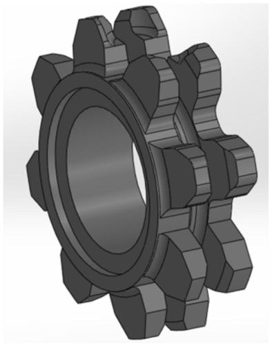
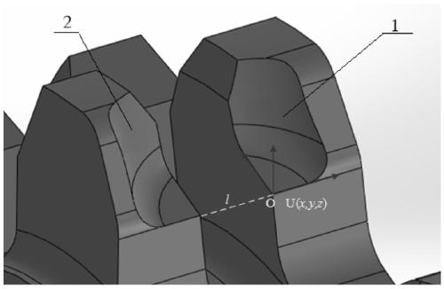
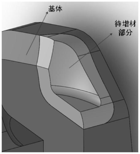
[0033] Specific implementation mode one: combine Figure 1 to Figure 16 To illustrate this embodiment, a mine sprocket sprocket socket surface automatic surfacing method described in this embodiment includes the following steps:
[0034] Step 1: Planning the walking path of the welding torch:
[0035] First obtain the curved surface information; then carry out multi-layer and multi-layer surfacing on the surface of the chain pocket; for a certain layer of surfacing welding, plan the welding torch vertical filling walking route on the surfacing surface to obtain discrete points; process the discrete points, Obtain the path point information of the weld bead on the final overall surface; determine the attitude information of the welding gun during the surfacing process of the robot; convert the obtained path point and attitude information into a robot execution program file;
[0036] Step 2: Use the line structured light sensor to determine the user coordinate system:
[0037]...
specific Embodiment approach 2
[0039] Specific implementation mode two: combination Figure 1 to Figure 16 To illustrate this embodiment, the process of obtaining curved surface information in Step 1 of this embodiment includes: before designing the surfacing path, firstly analyze the shape characteristics of the sprocket. Composed of gear teeth and a hollow hub, the shape of the chain socket is formed by the intersection of a curved surface and a plane. In order to represent the three-dimensional information of each chain socket surface, set the feature point O and the user coordinate system U(x, y, z), O select the chain socket The position of the intersection point of the two boundary lines of the plane part is extended along the two boundaries to be the X axis and the Y axis respectively, and the Z axis is determined according to the right-hand law to obtain the user coordinate system U(x,y,z), thus obtaining two symmetrically set chains Surface information of dimple surface 1 and chain dimple surface 2...
specific Embodiment approach 3
[0040] Specific implementation mode three: combination Figure 1 to Figure 16 To illustrate this embodiment, the process of multi-layer and multi-layer deposition on the surface of the chain socket in step 1 of this embodiment includes: using software to firstly perform equidistant curved surface processing on the surface of the chain socket that has not been surfacing, and point points on the curved surface of the chain socket Offset a specific distance along the normal phase vector direction of each point, and then filter and fit the new offset discrete points to obtain a surface with a specific offset distance from the initial chain nest surface Utilize contour faces that require surfacing Surface layer Trim, remove the part beyond the edge, and get the final surface that needs to be surfacing The undisclosed technical features in this embodiment are the same as those in the second embodiment.
[0041] In this embodiment, the solidworks software is used to firstly pr...
PUM
| Property | Measurement | Unit |
|---|---|---|
| thickness | aaaaa | aaaaa |
Abstract
Description
Claims
Application Information


