Back junction and back contact solar cell structure and preparation method thereof
A solar cell and back contact technology, applied in the field of solar cells, can solve the problems of high production cost and complicated process flow
- Summary
- Abstract
- Description
- Claims
- Application Information
AI Technical Summary
Problems solved by technology
Method used
Image
Examples
Embodiment
[0044] In order to make the above objects, features and advantages of the present invention more comprehensible, specific implementations of the present invention will be described in detail below in conjunction with the accompanying drawings.
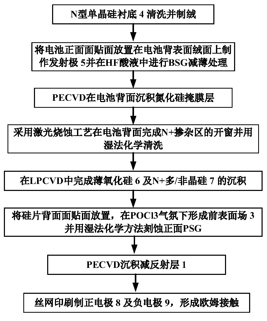
[0045] The patented technology of the present invention proposes a back-junction and back-contact solar cell structure and its preparation method. The cell structure includes from top to bottom: front anti-reflection layer (1) / passivation film (2), N+ doped layer (3) ), N-type silicon substrate (4), back P+ doped layer (5) and Topcon structure (ultra-thin oxide layer 6 and N+ poly / amorphous silicon 7) and battery electrodes: wherein, the battery electrodes include positive The electrode (8) and the negative electrode (9), the positive partial contact electrode is in contact with the P+ doped layer for deriving hole carriers; the negative partial contact electrode is in contact with N+ polysilicon or N+ amorphous silicon for deriving the...
PUM
| Property | Measurement | Unit |
|---|---|---|
| thickness | aaaaa | aaaaa |
| thickness | aaaaa | aaaaa |
Abstract
Description
Claims
Application Information

