Central surface acoustic wave heating element
A surface acoustic wave and heating element technology, which is applied in the field of central surface acoustic wave heating elements, can solve problems such as insufficient release of aroma and active ingredients, decline in electric heating performance of heating elements, and poor overall sensory quality, etc., to avoid sintering Adhesion, high heating efficiency, low heat generation effect
- Summary
- Abstract
- Description
- Claims
- Application Information
AI Technical Summary
Problems solved by technology
Method used
Image
Examples
Embodiment 1
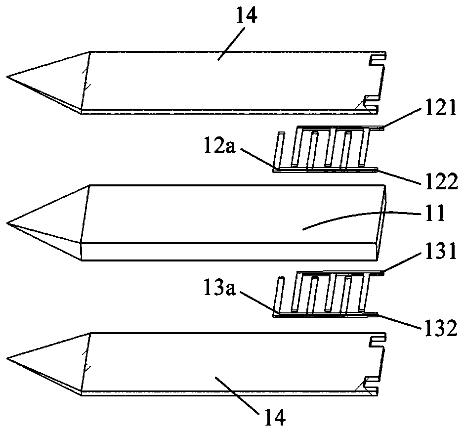
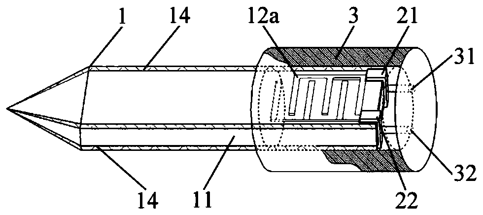
[0030] The structural schematic diagram and assembly effect diagram of the center-type surface acoustic wave heating element of this embodiment are shown in Figure 1 to Figure 3 , The central surface acoustic wave heating element is sword-shaped. The central surface acoustic wave heating element 1 includes a sword-shaped piezoelectric substrate 11, two interdigital electrode structures, respectively a first interdigital electrode structure 12a and a second interdigital electrode structure 13a, the two interdigital electrode structures Located on the upper and lower surfaces of the sword tail; the piezoelectric substrate 11, the first interdigitated electrode structure 12a, and the second interdigitated electrode structure 13a have a protective film layer 14, and the protective film material is generally silicon dioxide, Teflon , Parylene or SU8-2002 photoresist, etc., the thickness is preferably 1-3 μm, and this embodiment is 2 μm; the thickness of the sword tail is 0.5 mm, a...
Embodiment 2
[0033] Such as Figure 4 As shown, the front end of the central surface acoustic wave heating element in this embodiment is a conical rod. The central surface acoustic wave heating element 1 includes a rod-shaped piezoelectric substrate 11, and the two interdigital electrode structures are respectively the third interdigital electrode structure 12b and the fourth interdigital electrode structure 13b, the two interdigital electrode structures are located on the rod The periphery of the tail end; the surface of the piezoelectric substrate 11, the third interdigital electrode structure 12b, and the fourth interdigital electrode structure 13b has a protective film layer 14, the protective film material is the same as the embodiment, and the thickness is preferably 1-3 μm. This embodiment is also 2 μm; the perimeter of the rod tail end is 10mm; the material of the piezoelectric substrate 11 is the same as that of embodiment 1, and the interdigitated electrode structure of this embo...
PUM
| Property | Measurement | Unit |
|---|---|---|
| Thickness | aaaaa | aaaaa |
| Width | aaaaa | aaaaa |
| Perimeter | aaaaa | aaaaa |
Abstract
Description
Claims
Application Information


