Silicon carbide single crystal substrate
A silicon carbide single crystal and substrate technology, which is applied in the directions of single crystal growth, single crystal growth, crystal growth, etc., can solve the problem of not being able to fully alleviate changes, and achieve the effects of reliable manufacturing, improving quality, and reliable methods.
- Summary
- Abstract
- Description
- Claims
- Application Information
AI Technical Summary
Problems solved by technology
Method used
Image


Examples
no. 1 example
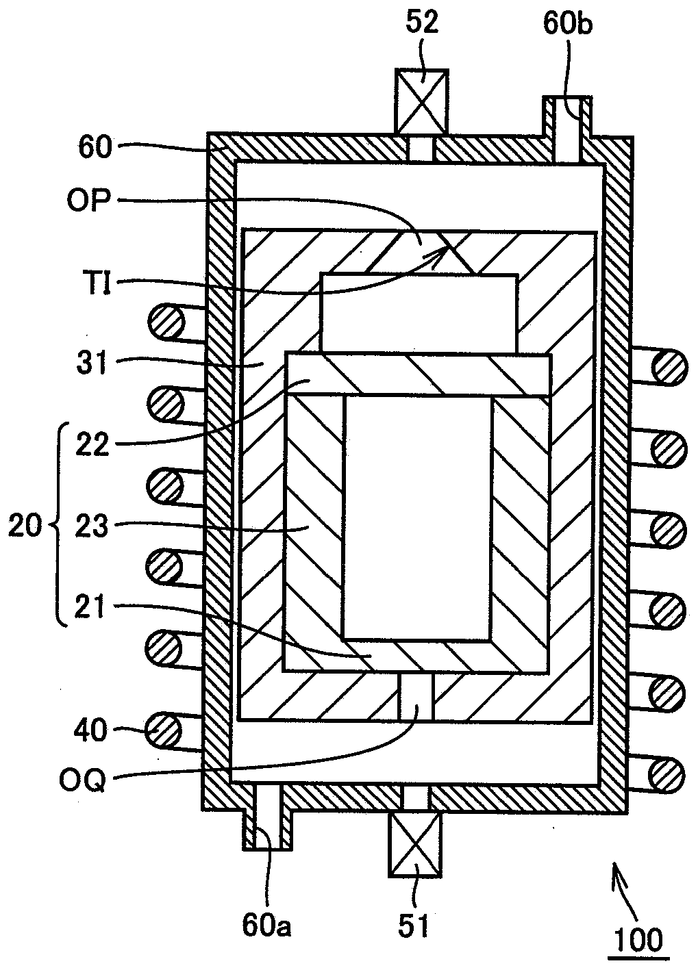
[0040] First refer to figure 1 A manufacturing apparatus 100 for a method of manufacturing an ingot (silicon carbide single crystal) in this embodiment is described. As will be described later, manufacturing apparatus 100 is an apparatus for growing a silicon carbide ingot using a sublimation recrystallization method. Manufacturing facility 100 has crucible 20 , heat insulating container 31 , external container 60 , heating section 40 , and radiation thermometers 51 and 52 .
[0041] The crucible 20 has a container portion including a bottom 21 (first side) and side portions 23, and a lid portion 22 (second side opposite to the first side). The container portion has a space for accommodating therein a solid source material for the sublimation recrystallization method. A lid portion 22 may be attached to a side portion 23 of the container portion to enclose the space. Furthermore, the lid portion 22 holds the seed crystal such that it is opposed to the space in the container...
no. 2 example
[0061] refer to Figure 9 , in this embodiment, a heat insulating container 32 is used to replace the heat insulating container 31 in the first embodiment ( figure 1 ). The heat insulating container 32 has a main body portion 32a and an outer portion 32b located outside the main body portion 32a. An opening OP in the heat insulating container 32 passes through the main body portion 32a and the outer side portion 32b. The opening OP has a tapered inner surface TI at the outer side 32b. The density of the outer portion 32b is higher than that of the main body portion 32a.
[0062] The main body portion 32a is preferably made of carbon fiber. The outer side portion 32b is preferably made of at least one of glassy carbon and pyrolytic carbon, and is more preferably made of glassy carbon or pyrolytic carbon. The surface roughness Ra of the tapered inner surface TI of the opening OP is preferably less than 0.9 μm, more preferably less than 0.7 μm, and further preferably less th...
no. 3 example
[0067] refer to Figure 10 , in this embodiment, a heat insulating container 33 is used to replace the heat insulating container 31 in the first embodiment ( figure 1 ). The opening OP in the heat insulating container 33 is such that the tapered inner surface TI and the cylindrical inner surface SI are connected to each other. The cylindrical inner surface SI is preferably arranged on the outside with respect to the conical inner surface TI. Therefore, the possibility of clogging of the cylindrical inner surface SI is less. Since features other than the above are substantially the same as those in the above-described first or second embodiment, the same or corresponding elements are assigned the same reference numerals, and description thereof will not be repeated.
PUM
| Property | Measurement | Unit |
|---|---|---|
| diameter | aaaaa | aaaaa |
| surface roughness | aaaaa | aaaaa |
Abstract
Description
Claims
Application Information
PatSnap Eureka turns technology decisions into work you can execute. Powered by our Innovation Knowledge Graph, it runs expert workflows across engineering, life sciences, materials and intellectual property. Get your review-ready output in minutes.


