Filling method of SiC epitaxial deep trench

A filling method and deep trench technology, applied in semiconductor devices, electrical components, circuits, etc., can solve problems affecting device leakage current and breakdown voltage, improve crystal quality, reduce density, and alleviate lattice mismatch Effect

Pending Publication Date: 2020-08-25
安徽长飞先进半导体有限公司
View PDF5 Cites 0 Cited by
  • Summary
  • Abstract
  • Description
  • Claims
  • Application Information

AI Technical Summary

Problems solved by technology

[0006] However, in the existing SiC epitaxial growth process, the interface dislocations formed between the substrate and the epitaxial layer and the defects on the substrate extend to the surface of the epitaxial layer, such as figure 2 As shown, it seriously affects the leakage current and breakdown voltage of the device

Method used


Image

  • Filling method of SiC epitaxial deep trench
  • Filling method of SiC epitaxial deep trench
  • Filling method of SiC epitaxial deep trench

Examples


Embodiment 1

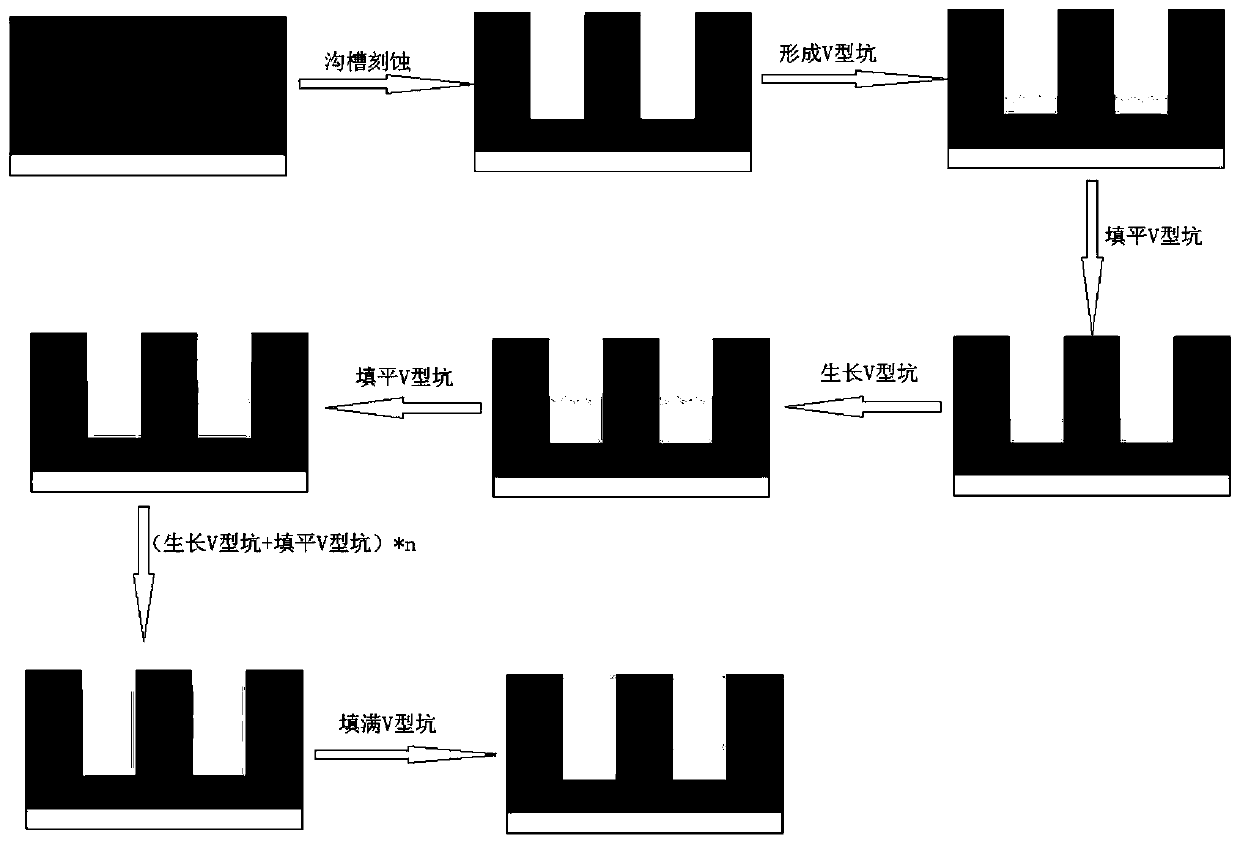
[0038] A method for filling a SiC epitaxial deep trench, comprising the following steps:

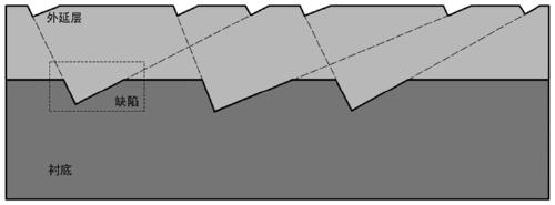
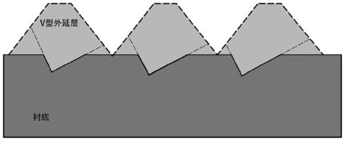
[0039] (1) 40-50 μm grown in epitaxial furnace, doping concentration 3×10 14 cm -3 ~9×10 16 cm -3N-type 4H-SiC epitaxial layer, take it out and clean it; groove etch the N-type 4H-SiC epitaxial layer grown on the substrate, the etching depth is greater than 10 μm along the crystal direction, and the groove side wall inclination angle 90°, the width of the bottom is consistent with the width of the top of the mesa, both are 1.5-2 μm, the mask is removed after etching; it is cleaned again, dried, and sent to the epitaxial furnace;

[0040] (2) Partially fill the etched trenches, and feed chlorine-containing silicon source gas, carbon source, HCl and Al doping at flow rates of 100-200 sccm, 100-200 sccm, 1000-5000 sccm and 20-50 sccm respectively agent, while passing H 2 and an inert gas such as helium or argon as a carrier gas, H 2 / The inert gas is 1~1 / 3, the total amount of carri...

Embodiment 2

[0046] A method for filling SiC epitaxial deep trenches, the others are the same as in Embodiment 1, except that between steps (1) and (2), a step of filling the intrinsic 4H-SiC buffer layer into the etched trenches is also included, The specific method is: close the N 2 For the dopant, an intrinsic SiC epitaxial layer with a thickness of 10-100 nm is grown as a buffer layer under the conditions for growing an N-type epitaxial layer.


PUM

PropertyMeasurementUnit
thicknessaaaaaaaaaa
thicknessaaaaaaaaaa
depthaaaaaaaaaa

Abstract

The invention provides a filling method of a SiC epitaxial deep trench. The method comprises the following steps: carrying out trench etching on an N-type 4H-SiC epitaxial layer grown on a substrate,wherein the etching depth is greater than 10 micrometers; partially filling the etched groove, and forming a SiC epitaxial layer with a V-shaped pit on the surface in the groove; filling and levelingup the V-shaped pit; repeating the steps for many times until the distance from the top of the trench is less than 5 micrometers; and filling the groove with a SiC epitaxial layer with a flat surfaceuntil the groove is filled. The transverse size of the V-shaped pit is reduced by controlling the growth condition; the V-shaped pit longitudinally grows at the initial stage; at the moment, the area(0001) is reduced; the defects can be fully turned, the probability that the dislocation penetrates to the surface is reduced, and the interface dislocation formed at the interface of the substrate and the epitaxial layer and the defects on the substrate are self-annihilated in the epitaxial growth process by utilizing the V-shaped pit defect self-annihilation mechanism, so that the leakage current of a device is reduced, and the breakdown voltage of the device is improved.

Description

technical field [0001] The invention belongs to the technical field of semiconductors, and relates to a method for filling a SiC epitaxial deep trench, in particular to a method for filling a SiC epitaxial deep trench with a depth greater than 10 μm. Background technique [0002] As a typical representative of the third-generation wide bandgap semiconductor materials, SiC has the characteristics of wide bandgap width, high critical breakdown field strength, high thermal conductivity and high carrier saturation rate. It has broad application prospects in the fields of energy saving and emission reduction, new energy vehicles, and smart grids. [0003] One of the important directions for the optimization and progress of SiC devices is to continuously reduce the specific on-resistance of the devices. The super junction technology is undoubtedly the most effective means to reduce the specific on-resistance of the drift region. Super junction technology is a technology that use...

Claims


Application Information

Patent Timeline
Patent Type & Authority Applications(China)
IPC IPC(8): H01L21/04H01L29/04H01L29/06H01L29/16
CPCH01L21/0475H01L21/0445H01L29/04H01L29/1608H01L29/0634H01L29/0684
Inventor 左万胜钮应喜刘洋张晓洪刘锦锦袁松章学磊史田超史文华钟敏胡新星
Owner 安徽长飞先进半导体有限公司
Why Eureka
Try Eureka