Wafer bonding structure and method

A technology for wafer bonding and bonding structure, applied in microstructure technology, microstructure device, manufacturing microstructure device, etc., can solve the problem of inability to accurately measure the wafer bonding deviation value.

Pending Publication Date: 2020-08-28
SHANGHAI HUAHONG GRACE SEMICON MFG CORP
View PDF8 Cites 2 Cited by
  • Summary
  • Abstract
  • Description
  • Claims
  • Application Information

AI Technical Summary

Problems solved by technology

[0005] The purpose of the present invention is to provide a wafer bonding structure and me...

Method used


Image

  • Wafer bonding structure and method
  • Wafer bonding structure and method
  • Wafer bonding structure and method

Examples


Embodiment Construction

[0040] A wafer bonding structure and method proposed by the present invention will be further described in detail below with reference to the accompanying drawings and specific embodiments. The advantages and features of the present invention will become clearer from the following description. It should be noted that all the drawings are in a very simplified form and use imprecise scales, and are only used to facilitate and clearly assist the purpose of illustrating the embodiments of the present invention. In addition, the structures shown in the drawings are often a part of the actual structures. In particular, each drawing needs to display different emphases, and sometimes uses different scales.

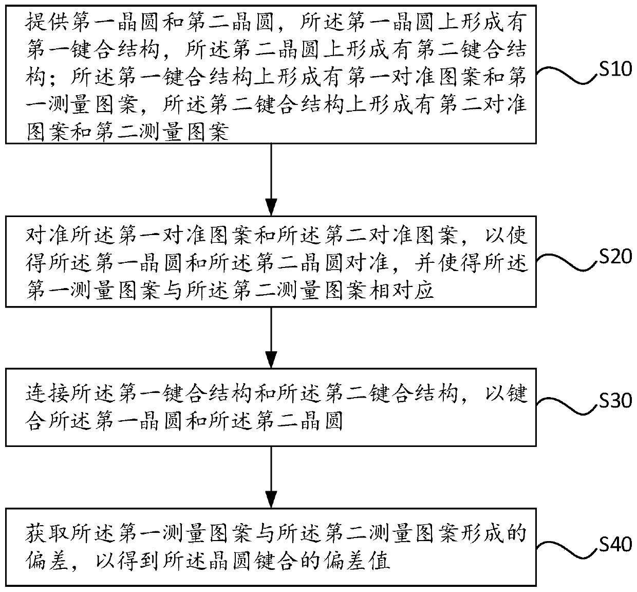
[0041] see figure 1 , the present embodiment provides a wafer bonding method, the wafer bonding method comprising:

[0042] Step 1 S10: providing a first wafer and a second wafer, the first bonding structure is formed on the first wafer, and the second bonding structure is form...


PUM


Abstract

The invention provides a wafer bonding structure and method, and the method comprises the following steps: providing a first wafer and a second wafer, forming a first bonding structure on the first wafer, and forming a second bonding structure on the second wafer, wherein a first alignment pattern and a first measurement pattern are formed on the first bonding structure, and a second alignment pattern and a second measurement pattern are formed on the second bonding structure. The first alignment pattern and the second alignment pattern are aligned, and the first measurement pattern corresponds to the second measurement pattern. And after the first wafer and the second wafer are bonded, a deviation formed by the first measurement pattern and the second measurement pattern is obtained so asto obtain a wafer bonding deviation value. According to the invention, the first measurement pattern and the second measurement pattern are additionally arranged on the first bonding structure and the second bonding structure respectively, so that the bonding deviation value can be directly read after wafer bonding, the process can be accurately monitored, a bonding machine can be calibrated, andthe yield of devices can be improved.

Description

technical field [0001] The invention relates to the technical field of semiconductor manufacturing, in particular to a wafer bonding structure and method. Background technique [0002] Micro-Electro-Mechanical Systems (MEMS) technology is known as a revolutionary high-tech in the 21st century. At present, highly integrated MEMS devices based on silicon, such as acceleration sensors and gyroscopes, are widely used in various fields such as industry, automobile, medical treatment, and military affairs. Among them, wafer bonding technology is one of the key technologies for the development and practical application of MEMS technology. [0003] Wafer bonding technology uses atoms on the surface of two wafers to react with each other and achieve a certain strength, so that the two wafers are bonded together. There are many methods for wafer bonding, such as fusion bonding, thermocompression bonding, low temperature vacuum bonding, anodic bonding, and eutectic bonding. Among th...

Claims


Application Information

Patent Timeline
IPC IPC(8): B81C1/00B81C3/00B81B7/02
CPCB81C1/00238B81C3/001B81C3/004B81B7/02
Inventor 徐爱斌王俊杰
Owner SHANGHAI HUAHONG GRACE SEMICON MFG CORP
Why Eureka
Try Eureka