Ceramic package shell and package shell mounting structure

A technology of ceramic packaging and housing, which is applied in the direction of semiconductor/solid-state device components, semiconductor devices, electrical components, etc., can solve the problems of high-density and interconnection of microwave packaging housings, achieve excellent microwave performance, and increase wiring density , the effect of high-density wiring

Active Publication Date: 2021-12-24
THE 13TH RES INST OF CHINA ELECTRONICS TECH GRP CORP
View PDF1 Cites 1 Cited by
  • Summary
  • Abstract
  • Description
  • Claims
  • Application Information

AI Technical Summary

Problems solved by technology

[0004] The purpose of the present invention is to provide a ceramic packaging shell, which aims to solve the technical problem that the existing microwave packaging shell cannot perform high-density interconnection

Method used


Image

  • Ceramic package shell and package shell mounting structure
  • Ceramic package shell and package shell mounting structure
  • Ceramic package shell and package shell mounting structure

Examples


Embodiment Construction

[0034] In order to make the technical problems, technical solutions and beneficial effects to be solved by the present invention clearer, the present invention will be further described in detail below in conjunction with the accompanying drawings and embodiments. It should be understood that the specific embodiments described here are only used to explain the present invention, not to limit the present invention.

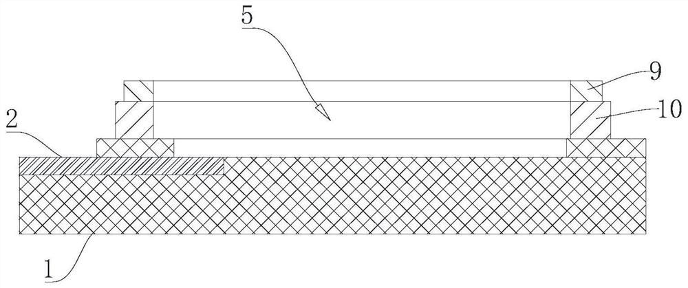
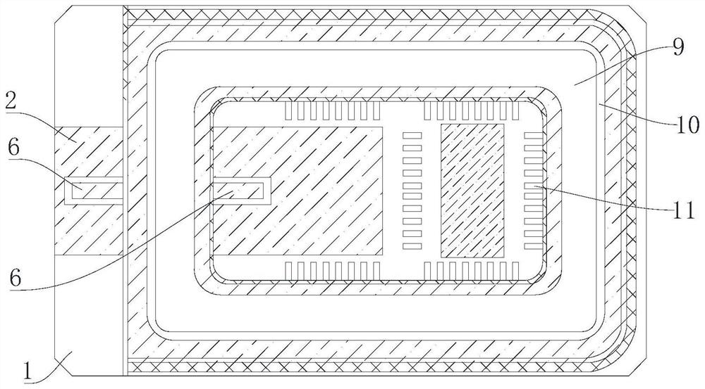
[0035] Please also refer to Figure 1 to Figure 5 , the ceramic packaging shell provided by the present invention will now be described. The ceramic packaging shell includes a ceramic base 1, a ceramic insulator 2, a cover plate 3 and a pad structure; the ceramic base 1 is a multi-layer structure, and the ceramic base 1 is provided with a cavity 5 with an upward opening; the ceramic insulator 2 is arranged on a ceramic On the substrate 1, a radio frequency transmission structure 6 is formed on the upper part of the ceramic insulator 2, and the radio frequency tran...


PUM


Abstract

The invention provides a ceramic packaging shell, which belongs to the technical field of chip packaging, and includes a ceramic substrate, a ceramic insulator, a cover plate and a pad structure; the ceramic substrate is a multi-layer structure and is provided with a cavity; the ceramic insulator is arranged on the ceramic substrate, The upper part has a radio frequency transmission structure set through the side wall of the cavity; the sealing cover of the cover plate is set on the cavity; the welding pad structure is set on the bottom of the ceramic substrate. The ceramic package shell provided by the invention enables the package shell to have excellent microwave performance, high-density wiring, highly integrated component distribution and a larger number of leads, enabling high-density interconnection. The present invention also provides a package housing installation structure, the circuit board is provided with a first stepped structure whose upper surface is flush with the upper surface of the ceramic insulator, the first stepped structure is provided with a bonding structure for connecting with the radio frequency transmission structure, the circuit board A circuit board pad structure welded to the pad structure is provided on the top. It facilitates mounting with ceramic package housings while ensuring impedance matching.

Description

technical field [0001] The invention belongs to the technical field of chip packaging, and more specifically relates to a ceramic package shell and a package shell mounting structure. Background technique [0002] With the continuous development of microwave semiconductor technology, the operating frequency of the device is getting higher and higher, which requires the packaging shell to adapt to the packaging of higher frequency devices and smaller standing waves. The metal cavity embedded ceramic insulator structure shell is suitable for packaging more It is an ideal packaging shell form for high-frequency devices. It can seal one or more microwave and millimeter-wave semiconductor chips in a separate box, and realize the interconnection of microwave signals with external circuits through ceramic insulators as input and output terminals. Because the entire shell It is a fully sealed structure, which isolates the erosion of the chip by the external environment, and the devi...

Claims


Application Information

Patent Timeline
Patent Type & Authority Patents(China)
IPC IPC(8): H01L25/18H01L23/31H01L23/488
CPCH01L25/18H01L23/3128H01L24/14H01L2224/1413H01L2224/48091H01L2924/00014H01L2224/48227H01L2924/15311H01L2924/19107H01L2924/171H01L2924/16195H01L24/48H01L2924/165H01L2924/3011H01L2924/20271H01L2924/3512H01L23/66H01L2223/6611H01L2223/6633H01L2223/6655H01L23/053H01L23/49838H01L23/15H01L23/49816H01L2224/45099H01L23/13H01L23/49822H01L23/49833H01L25/0655H01L2223/6627H01L2224/48155H01L2224/48225H01L2924/16251H01L2924/1631H01L2924/1632
Inventor 杨振涛
Owner THE 13TH RES INST OF CHINA ELECTRONICS TECH GRP CORP
Why Eureka
Try Eureka