Heterogeneous integrated structure of two-dimensional material device and GaN device and preparation method

A technology of two-dimensional materials and devices, which is applied in the field of heterointegrated structure and preparation of two-dimensional material devices and GaN devices, can solve the problems of difficulty in exerting the advantages of GaN devices and low performance of combined devices, so as to solve the problem of poor ohmic contact and reduce parasitics. effect, effect of shortening distance

Active Publication Date: 2020-08-28
ZHEJIANG UNIV
View PDF5 Cites 3 Cited by
  • Summary
  • Abstract
  • Description
  • Claims
  • Application Information

AI Technical Summary

Problems solved by technology

[0005] In view of the shortcomings of the prior art described above, the purpose of the present invention is to provide a heterogeneous integrated structure and preparation method of a two-dimensional materia

Method used


Image

  • Heterogeneous integrated structure of two-dimensional material device and GaN device and preparation method
  • Heterogeneous integrated structure of two-dimensional material device and GaN device and preparation method
  • Heterogeneous integrated structure of two-dimensional material device and GaN device and preparation method

Examples


Embodiment Construction

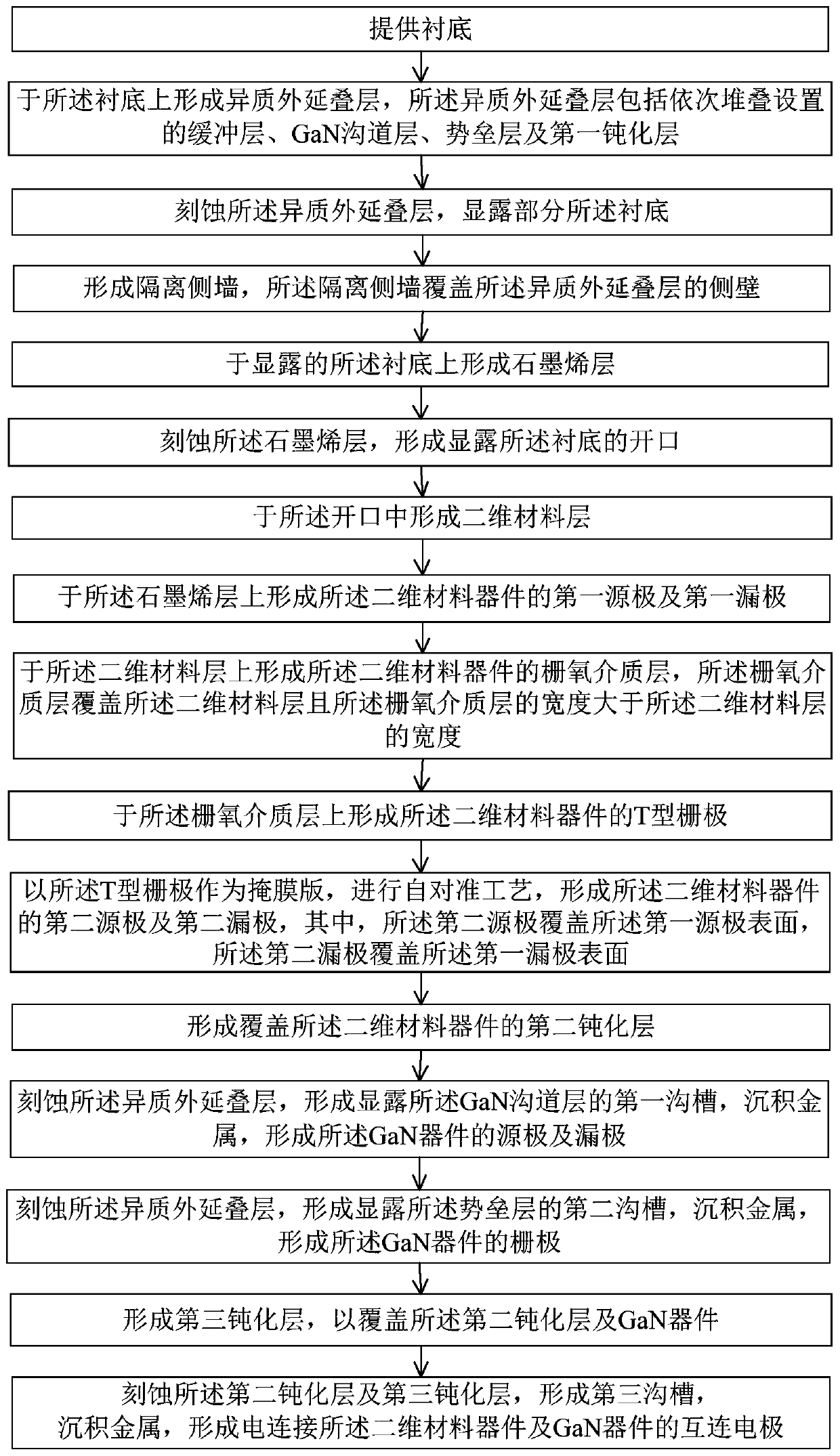
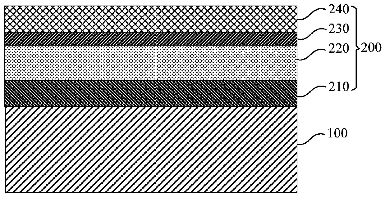
[0069] Embodiments of the present invention are described below through specific examples, and those skilled in the art can easily understand other advantages and effects of the present invention from the content disclosed in this specification. The present invention can also be implemented or applied through other different specific implementation modes, and various modifications or changes can be made to the details in this specification based on different viewpoints and applications without departing from the spirit of the present invention.

[0070] see Figure 1 to Figure 16 . It should be noted that the diagrams provided in this embodiment are only schematically illustrating the basic idea of ​​the present invention, so only components related to the present invention are shown in the drawings rather than the number, shape and shape of components in actual implementation. Dimensional drawing, the type, quantity and proportion of each component can be changed arbitrarily...


PUM


Abstract

The invention provides a heterogeneous integrated structure of a two-dimensional material device and a GaN device and a preparation method. The two-dimensional material device and the GaN device are heterogeneously integrated on the same sapphire substrate, on and off of the GaN device are controlled through the two-dimensional material device, the performance of the overall heterogeneous integrated structure is improved, and the advantages of the GaN device are exerted; electric connection is achieved through interconnection electrodes, and the parasitic effect is reduced; in the two-dimensional material device, a two-dimensional material layer is used as a channel, a graphene layer is used as ohmic contact, and the problem of poor ohmic contact of the two-dimensional material device is solved; and a T-shaped grid electrode is used as a mask plate and a self-alignment process is carried out to form a second source electrode and a second drain electrode, so that the distances between the T-shaped grid electrode and the source electrode and between the T-shaped grid electrode and the drain electrode are shortened, the access resistance of the two-dimensional material device is reduced, and the performance of the two-dimensional material device is improved. According to the invention, the advantages of the GaN device can be fully exerted, and the performance of the whole heterogeneous integrated structure is improved.

Description

technical field [0001] The invention belongs to the technical field of semiconductors, and relates to a heterogeneous integration structure and a preparation method of a two-dimensional material device and a GaN device. Background technique [0002] As a representative of the third-generation semiconductor materials, gallium nitride (GaN) has many excellent characteristics such as high critical breakdown electric field, high electron mobility, high two-dimensional electron gas concentration, and good high-temperature working ability. Therefore, GaN-based third-generation semiconductor devices, such as high electron mobility transistors (HEMTs) and heterojunction field effect transistors (HFETs), have been applied, especially in fields requiring high power and high frequency such as radio frequency and microwave. has obvious advantages. [0003] Conventional GaN HEMT devices are normally-on devices. The most direct way to realize the normal shutdown of GaN HEMT devices is to...

Claims


Application Information

Patent Timeline
IPC IPC(8): H01L29/10H01L29/20H01L29/24H01L29/778H01L29/78H01L21/335H01L21/336
CPCH01L27/0617H01L29/1029H01L29/2003H01L29/24H01L29/66462H01L29/66477H01L29/778H01L29/78
Inventor 莫炯炯王志宇陈华刘家瑞郁发新
Owner ZHEJIANG UNIV
Why Eureka
Try Eureka