LED display screen module and preparation method thereof

A LED display and LED chip technology, applied in electrical components, electrical solid devices, circuits, etc., can solve the problems of inconsistent ink color of unit boards/modules, uneven mixing of melanin/powder, uneven color and brightness, etc., to reduce mixing light phenomenon, reduce virtual welding or desoldering or damage, and solve the effect of color difference

Pending Publication Date: 2020-08-28
HCP TECH CO LTD
View PDF5 Cites 12 Cited by
  • Summary
  • Abstract
  • Description
  • Claims
  • Application Information

AI Technical Summary

Problems solved by technology

[0003] At present, LED displays mainly use PCB (including FR4, FR4+ type BT, BT type or FPC) or Glass as the display substrate to complete the small pitch (Pitch≤2.5mm) display screen. As for the packaging method: One of them is to use the traditional package + SMD to complete the LED display light board, and the other is to use COB (Chip on Board) to bond the R, G, and B flip chips on the PCB board, and then Epoxy resin (EPOXY)/silica gel + melanin/color paste/toner is molded on the surface of the LED chip by compression molding to protect the LED chip and reduce the brightness, but it also has the following disadvantages: 1. .

Method used


Image

  • LED display screen module and preparation method thereof
  • LED display screen module and preparation method thereof
  • LED display screen module and preparation method thereof

Examples


Embodiment 1

[0045] Such as Figure 1 to Figure 5 As shown, the present embodiment provides a method for preparing an LED display module, the method comprising:

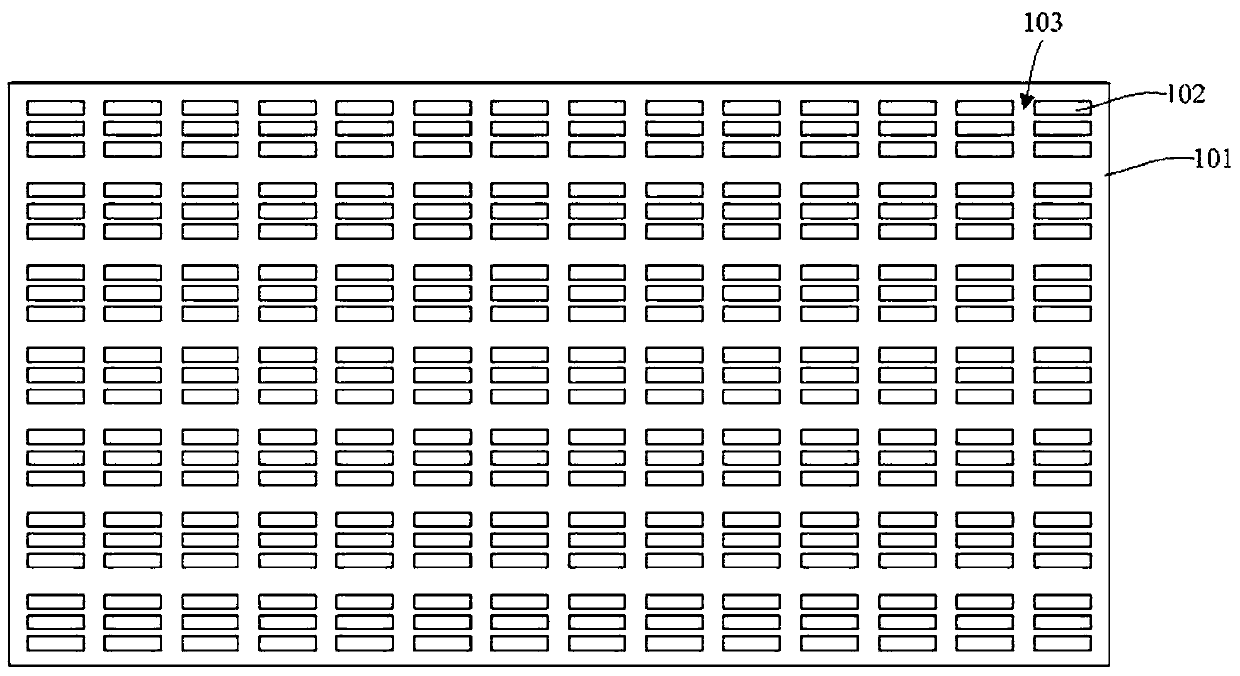
[0046] Such as figure 1 As shown, step 1) is first performed, and the LED display module including the LED chip array is fixed on the jig, and the LED chip array is placed upward.

[0047] The LED display module includes: a substrate 101 ; an array of LED chips disposed on the front of the substrate 101 . The substrate 101 may be one of a PCB substrate or a glass substrate. In this embodiment, the substrate 101 is a PCB substrate. The substrate also includes thin film transistors (TFTs). Optionally, there is an electrode array on the front surface of the substrate. Optionally, the back of the substrate is connected to a driver chip and a connector, and the driver chip and connector are arranged on the back of the substrate 101

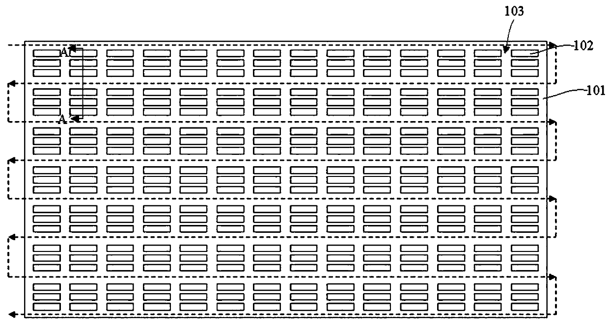
[0048] The LED chip array includes a plurality of regularly arranged LED chips 102, and the LED...

Embodiment 2

[0079] Such as Figure 7 As shown, this embodiment provides a method for preparing an LED display module, the basic steps of the preparation method are as in Example 1, and the difference from Example 1 is:

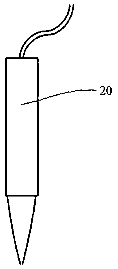
[0080] Step 2) Apply glue on the center line of the gap 103 of the LED chip 102 using a single-needle gluer 20, apply glue longitudinally from one corner of the LED display module substrate to the edge of the other end, and then change the direction by 90° to the other end. For a row of starting points, change the direction by 90° again and apply glue along the dotted line, then apply glue to the following starting points, and apply glue to all partitions in this way.

[0081] This embodiment also provides an LED display module, the difference between the module and Embodiment 1 is:

[0082] The substrate 101 is a glass substrate, and the substrate further includes a thin film transistor (TFT) layer. Optionally, there is an electrode array on the front surface of the subs...

Embodiment 3

[0084] Such as Figure 8 and Figure 9 As shown, this embodiment provides a method for preparing an LED display module, the basic steps of the preparation method are as in Example 1, and the difference from Example 1 is:

[0085] Step 2) Apply glue on the center line of the gap 103 of the LED chip 102 using a multi-needle gluer 30. The gap between the needles of the gluer is consistent with the gap to be glued, as Figure 8 shown. Apply glue from the left side of the LED display module substrate to the edge of the other end, then rotate it 180° downwards, adjust the position to the starting point on the right, apply glue along the dotted line to the left edge of the LED display module, and apply this method cyclically Glue to all partitions like Figure 9 shown.

[0086] In this embodiment, a multi-needle gluing machine is used to apply glue, which can simultaneously apply glue to the gaps 103 of multiple LED chips 102 , which greatly reduces the time required for glue app...


PUM

PropertyMeasurementUnit
Thicknessaaaaaaaaaa
Thicknessaaaaaaaaaa

Abstract

The invention provides an LED display screen module and a preparation method thereof. The preparation method comprises the steps: 1) fixing a LED display screen module comprising an LED chip array toa jig, wherein the LED chip array is placed upwards; 2) injecting a black filling glue solution into gaps between the LED chips; 3) solidifying the black filling glue solution; 4) forming a transparent packaging layer; and 5) forming an ink color layer on the transparent packaging layer. According to the invention, by combining a transparent packaging layer and an ink color layer, the thickness ofthe ink color layer is greatly reduced compared with that of a traditional pressing mold layer, so that the path change of light passing through the ink color layer under different-angle emergence can be reduced, and the defect that the light emitting brightness and color of the display screen module change along with the viewing angle is reduced; and the thickness of the ink color layer is 5-200microns, the brightness of the display screen module can be effectively reduced to be within the brightness range acceptable to human eyes, and a comfortable visual brightness interval is shaped.

Description

technical field [0001] The invention belongs to the field of semiconductor display design and manufacture, in particular to an LED display module and a preparation method thereof. Background technique [0002] The continuous development of society and the vigorous advocacy of the country have made the LED industry one of the most active industries today, and LED display products have gradually entered various fields of society and life. At the same time, with the innovation and development of LED display technology, the small-pitch seamless connection LED display module with high resolution per unit area has become the mainstream product of LED display, which can display higher-definition graphics and images. Video can also display more video and image images, especially in the application of image stitching, which can achieve seamless and arbitrary large-area stitching. [0003] At present, LED displays mainly use PCB (including FR4, FR4+ type BT, BT type or FPC) or Glass ...

Claims


Application Information

Patent Timeline
IPC IPC(8): H01L33/44H01L33/52H01L33/56H01L33/58H01L25/075
CPCH01L33/52H01L33/56H01L33/58H01L33/44H01L25/0753H01L2933/0025H01L2933/005H01L2933/0058
Inventor 黄志强庄文荣孙明付小朝卢敬权蒙健佳
Owner HCP TECH CO LTD
Why Eureka
Try Eureka