LED optical system of DI photoetching machine

An optical system and lithography machine technology, applied in the field of lithography, can solve the problems of low energy, high price, and single wavelength, and achieve the effects of low energy consumption, low manufacturing cost, and concentrated beam

Pending Publication Date: 2020-09-01
广东科视光学技术股份有限公司
View PDF0 Cites 6 Cited by
  • Summary
  • Abstract
  • Description
  • Claims
  • Application Information

AI Technical Summary

Problems solved by technology

However, most of the light sources used in DI lithography machines are ultraviolet semiconductor lasers. This type of ultraviolet semiconductor lasers is expensive, has low energy, and has a single wavelength.

Method used


Image

  • LED optical system of DI photoetching machine
  • LED optical system of DI photoetching machine
  • LED optical system of DI photoetching machine

Examples


Embodiment Construction

[0017] The following will clearly and completely describe the technical solutions in the embodiments of the present invention with reference to the accompanying drawings in the embodiments of the present invention. Obviously, the described embodiments are only some, not all, embodiments of the present invention. Based on the embodiments of the present invention, all other embodiments obtained by persons of ordinary skill in the art without making creative efforts belong to the protection scope of the present invention.

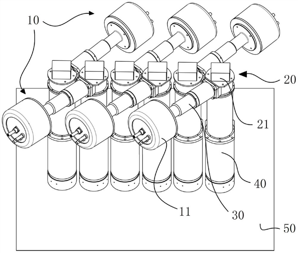
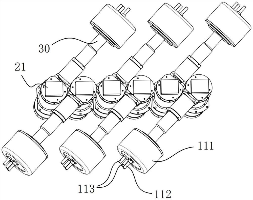
[0018] figure 1 It is a structural schematic diagram of an LED optical system of a DI lithography machine in an embodiment, figure 2 for figure 1 The top view; the LED optical system of this DI lithography machine includes a near ultraviolet LED light source module 10, a condenser lens 30, a photolithography module 20 and an imaging lens 40, the near ultraviolet LED light source module 10, a condenser lens 30 , the lithography module 20 and the imaging lens...


PUM


Abstract

The invention discloses an LED optical system of a DI photoetching machine. The LED optical system comprises a near ultraviolet LED luminous source module, a condensing lens, a photoetching module andan imaging lens, the near ultraviolet LED luminous source module comprises a plurality of near-ultraviolet LED light-emitting sources, each near-ultraviolet LED light-emitting source is connected with the photoetching module through a condensing lens, and the plurality of near-ultraviolet LED light-emitting sources are arranged on two sides of the photoetching module in a staggered manner; the photoetching module comprises a plurality of DMD photoetching devices which are linearly arranged, one end of each DMD photoetching device is connected with the imaging lens, and the other end of each DMD photoetching device is connected with the condensing lens; an included angle between a straight line where the near ultraviolet LED light-emitting source and the DMD photoetching devices are located and a straight line where the plurality of DMD photoetching devices are located is less than 90 degrees; and a plurality of near-ultraviolet LED luminous bodies are arranged in the near-ultravioletLED light-emitting source. The invention solves the problems of insufficient power of some wavebands of the existing semiconductor laser and low energy of the small LED composite light source, and hasthe advantages of the simple structure, low energy consumption, the low manufacturing cost and the stable performance.

Description

technical field [0001] The invention relates to the technical field of photolithography used for PCB board manufacturing, in particular to an optical system of a direct imaging DI photolithography machine applied to exposure equipment. Background technique [0002] In both the wafer manufacturing industry and the PCB manufacturing industry, photolithography and etching processes are required to complete the generation of design graphics on wafers or copper-clad boards, so as to realize the functions of various devices or circuits. The traditional photolithography process requires the use of pre-fabricated reticles or negatives to be exposed through photolithography machines for pattern transfer. Making reticles or negatives not only increases production costs, but also lengthens the production cycle. With the advancement of exposure technology, a new exposure technology DI or LDI (Laser Direct Imaging) is becoming more and more mature. This technology can directly project th...

Claims


Application Information

Patent Timeline
Patent Type & Authority Applications(China)
IPC IPC(8): G03F7/20
CPCG03F7/2004G03F7/7005G03F7/7015
Inventor 王华吴中海陈志特冯明瑞
Owner 广东科视光学技术股份有限公司
Why Eureka
Try Eureka