

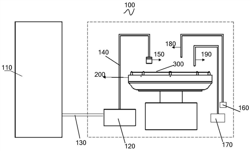
Photoresist removing device and method for removing photoresist
A photoresist and nano-bubble technology, applied in the field of photoresist removal and photoresist removal device, can solve the problems of high cost, high sulfuric acid consumption, device damage, etc., meet the requirements, improve the removal efficiency, and reduce the production cost cheap effect
- Summary
- Abstract
- Description
- Claims
- Application Information
AI Technical Summary
Problems solved by technology
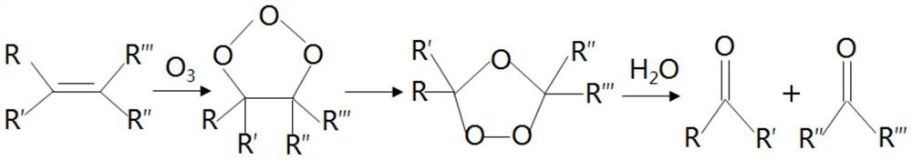
Method used
Image

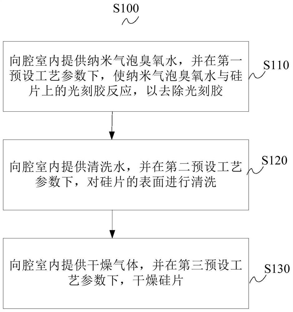
Examples
Embodiment 1
[0078] In this embodiment, nanobubble ozone water O 3 The concentration of is 20ppm, the vertical distance between the first shower head and the silicon wafer is 15mm, the swing speed of the second end of the nanobubble pipeline is 8rpm, and the remaining process parameters of photoresist cleaning are shown in Table 1:
[0079]
[0080] Table 1 Photoresist cleaning process parameters
Embodiment 2
[0082] In this embodiment, nanobubble ozone water O 3 The concentration is 50ppm, the vertical distance between the first shower head and the silicon wafer is 20mm, the swing speed of the second end of the nanobubble pipeline is 8rpm, and the rest of the photoresist cleaning process parameters are shown in Table 2:
[0083]
[0084] Table 2 Photoresist cleaning process parameters
PUM
 Abstract
Description
Claims
Application Information