
Packaging crystal back grinding structure and grinding method

A grinding method and crystal back technology, which is applied in the direction of grinding devices, grinding machine tools, measuring devices, etc., can solve the problems that the double-sided adhesive cannot be firmly pasted, the observation effect cannot be achieved, and the crystal back grinding is easy to fail, etc., and the structure is simple, Reduce the unevenness of the corners of the back of the crystal and prevent the sample from falling

Pending Publication Date: 2020-09-01
苏试宜特(深圳)检测技术有限公司
View PDF6 Cites 7 Cited by
  • Summary
  • Abstract
  • Description
  • Claims
  • Application Information

AI Technical Summary

Problems solved by technology

Smaller samples cannot be firmly adhered to the double-sided adhesive tape during crystal back grinding, and they tend to fall off during grinding, resulting in poor flatness and easy failure of crystal back grinding
In addition, when the CSP (Chip Scale Package, chip scale package) package sample is ground on the crystal back, due to the unevenness around the chip, the desired observation effect cannot be achieved.

Method used


Image

  • Packaging crystal back grinding structure and grinding method
  • Packaging crystal back grinding structure and grinding method

Examples


Embodiment Construction

[0028] Embodiments of the present invention are described below through specific examples, and those skilled in the art can easily understand other advantages and effects of the present invention from the content disclosed in this specification. The present invention can also be implemented or applied through other different specific implementation modes, and various modifications or changes can be made to the details in this specification based on different viewpoints and applications without departing from the spirit of the present invention.

[0029] The embodiments of the present invention will be described in further detail below in conjunction with the accompanying drawings and specific embodiments.

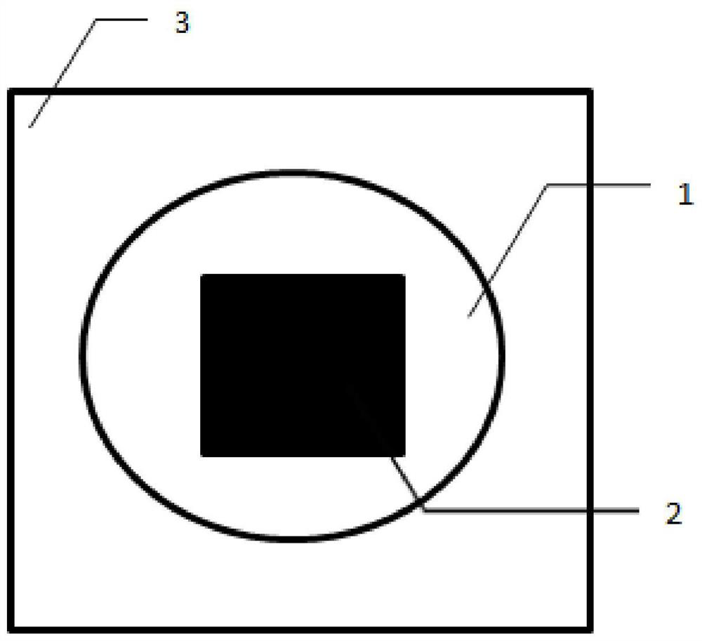
[0030] combine figure 1 with figure 2 As shown, the embodiment of the present invention provides an advanced packaging crystal back grinding method, which can be used for hot spot positioning equipment, which mainly includes the following steps:

[0031] (1) Configure gl...


PUM


Abstract

The invention discloses a packaging wafer back grinding structure and a grinding method. The grinding method comprises the steps of preparing a glue; preparing a sample; taking a piece of cover glassand adhering the cover glass to an adhesive tape; dropwise adding the prepared glue on the cover glass, slowly putting the sample into the glue until the sample is completely immersed in the glue, lightly pressing the sample to discharge bubbles at the bottom of the sample, standing, observing whether bubbles are generated or not, puncturing the generated bubbles and then putting the sample on a heating table for baking so as to obtain the prepared sample; carrying out the post-treatment; after the sample is cooled, removing the adhesive tape, grinding off the redundant cover glass, adjustingthe cover glass to the proper size, and starting the packaging crystal back grinding. The packaging wafer back grinding structure is simple and is convenient in sample preparation, by the A and B gluepreparation, the stress on the sample is reduced, the flatness during grinding is kept, and the grinding area is increased. The packaging wafer back grinding structure has the advantages of high sample preparation success rate, better observation effect and the like.

Description

technical field [0001] The invention relates to a method for manufacturing a semiconductor integrated circuit, in particular to a packaging crystal back grinding structure and a grinding method. Background technique [0002] Semiconductor chips often fail during research and development, mass production, and consumer use. With the rapid development of electronic science and technology and the continuous improvement of integration, semiconductor chips are becoming more and more complex, and people's requirements for product quality and reliability are constantly increasing. However, failure analysis technology is closely related to quality and reliability, which shows the importance of failure analysis technology. Through chip failure analysis, IC designers can help IC designers find design defects, process parameters that do not comply with regulations, or improper operation. [0003] In general, when performing hotspot positioning, some chips often choose to perform posit...

Claims


Application Information

Patent Timeline
Patent Type & Authority Applications(China)
IPC IPC(8): H01L21/02B24B37/34G01N1/28G01N1/36G01N1/44G01R31/28
CPCH01L21/02013H01L21/02016G01N1/36G01N1/44G01N1/286G01R31/2898B24B37/34G01N2001/364G01N2001/2866
Inventor 李延昭原岩峰
Owner 苏试宜特(深圳)检测技术有限公司
Learn More