

Display panel and display device
A display panel and substrate technology, applied to electrical components, transistors, diodes, etc., can solve problems such as lower product yield, breakdown of thin lines, and poor product reliability
- Summary
- Abstract
- Description
- Claims
- Application Information
AI Technical Summary
Problems solved by technology
Method used
Image

Examples
Embodiment Construction
[0027] In order to make the purpose, technical solutions and advantages of the embodiments of the present invention more clear, various implementation modes of the present invention will be described in detail below in conjunction with the accompanying drawings. However, those of ordinary skill in the art can understand that in each implementation manner of the present invention, many technical details are proposed in order to enable readers to better understand the present invention. However, even without these technical details and various changes and modifications based on the following implementation modes, the technical solution claimed in the present invention can also be realized.
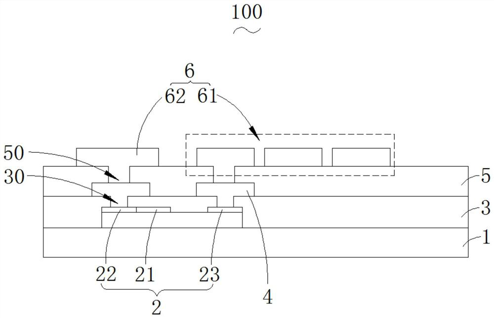
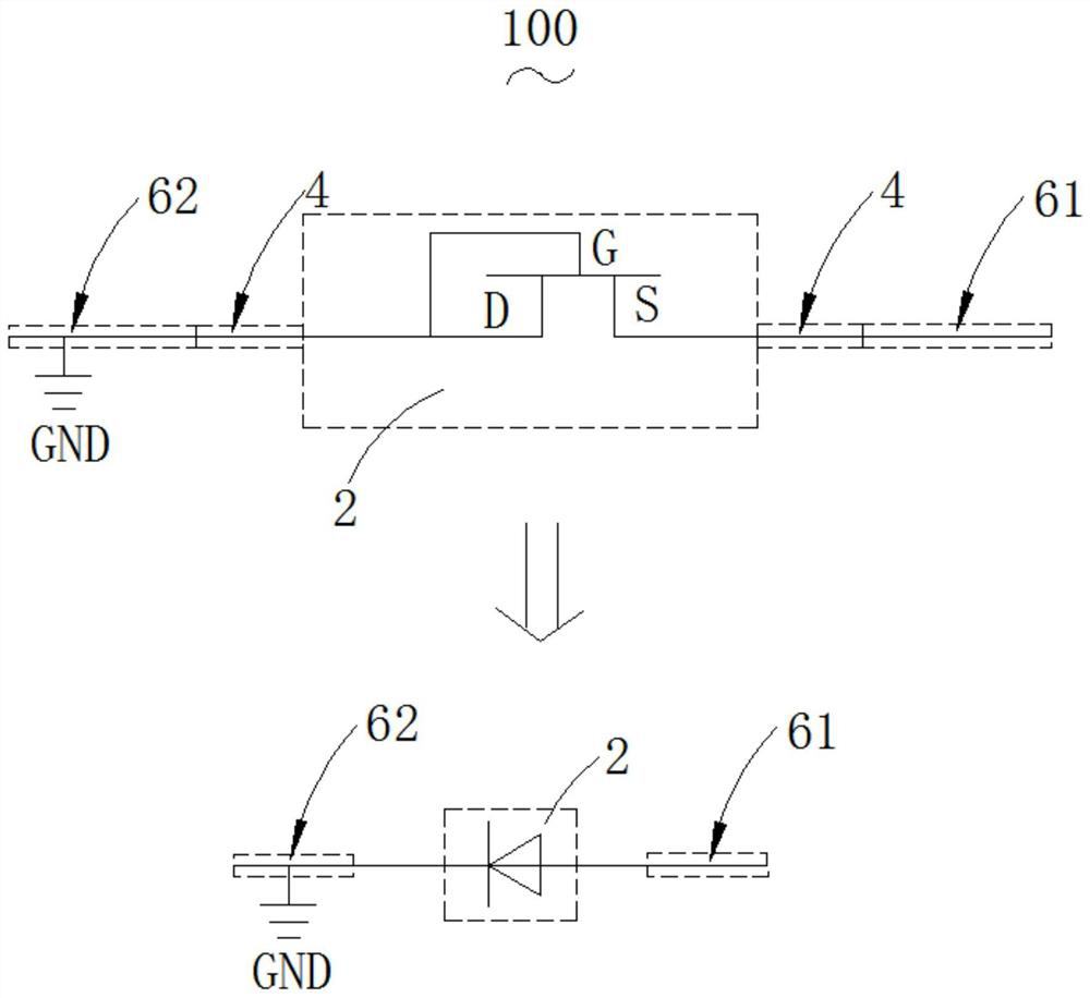
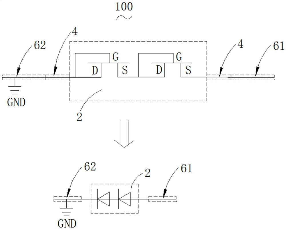
[0028] The first embodiment of the present invention relates to a display panel 100, the specific structure is as follows figure 1 and figure 2 shown, including:
[0029] The substrate 1; the MOS transistor 2, the MOS transistor 2 is arranged on the substrate 1, and the gate 21 and the dr...
PUM
| Property | Measurement | Unit |
|---|---|---|
| thickness | aaaaa | aaaaa |
| thickness | aaaaa | aaaaa |
Abstract
Description
Claims
Application Information