

Extended EDAC check circuit and read-write method for extended Flash program storage area
Patent Information
- Authority / Receiving Office
- CN · China
- Patent Type
- Applications(China)
- Current Assignee / Owner
- XIAN MICROELECTRONICS TECH INST
- Publication Date
- 2020-09-18
Smart Images
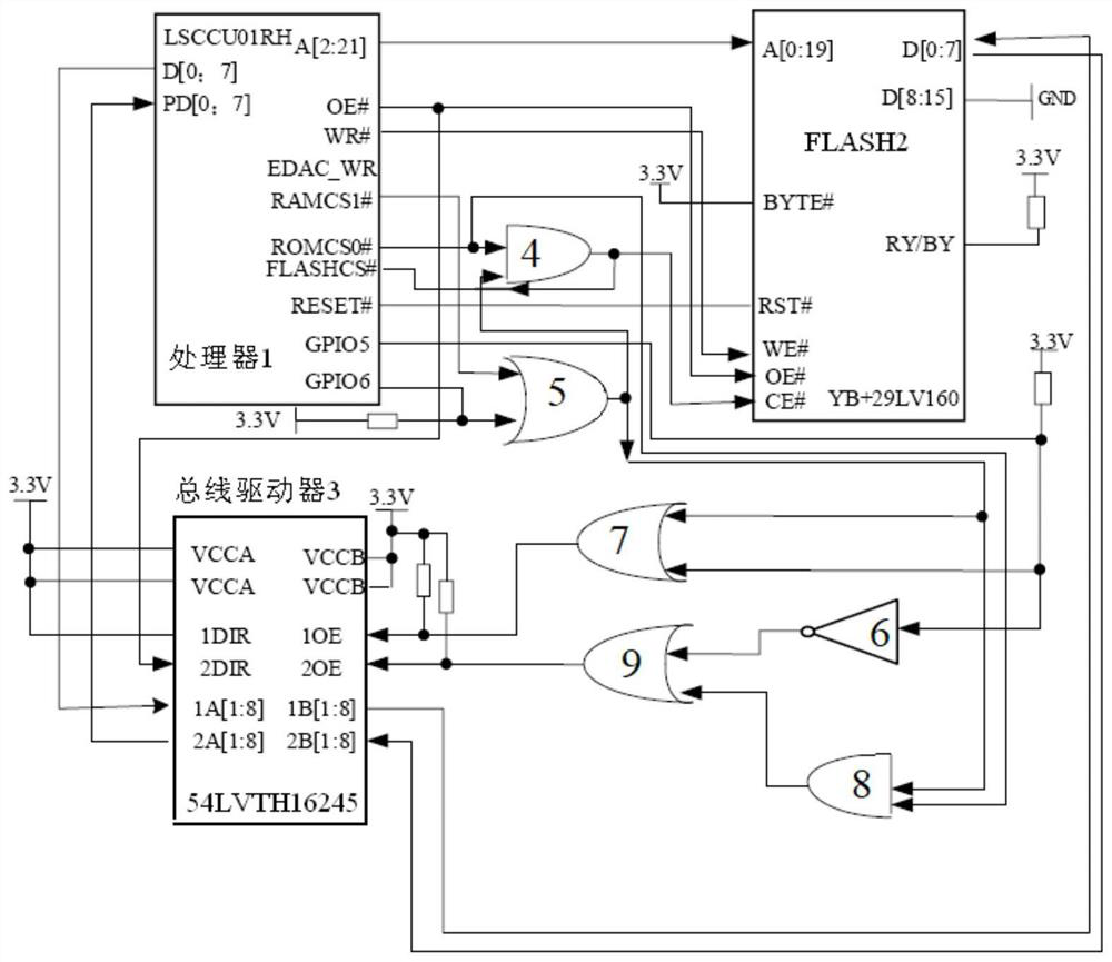
Figure 1 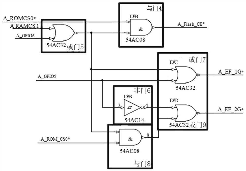
Figure 2 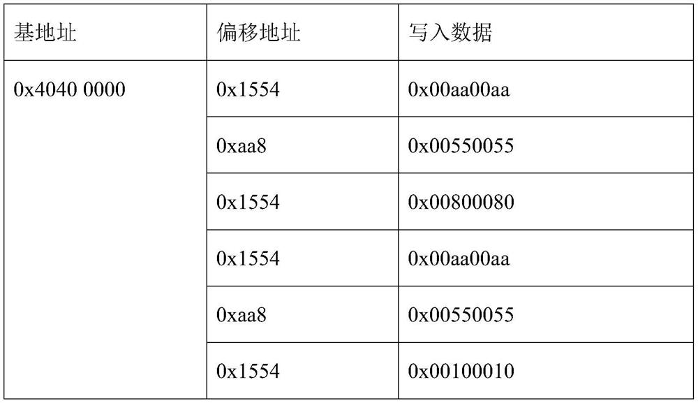
Figure 3
Abstract
Description
technical field
[0001] The invention belongs to the application field of space embedded computers, and in particular relates to an externally expanded Flash program storage area expanded EDAC verification circuit and a reading and writing method. Background technique
[0002] Miniaturization is the development trend of space embedded computers. At present, the processor system and functional modules in the computer are built with discrete components, which are large in size and heavy in weight. The development and application of SIP technology provides technical support for the miniaturization design of space embedded computer. The SIP module LSCCU01RH, which has been applied and successfully flown on the space computer, has greatly reduced the size, weight, and power consumption of the computer, and the module works stably, performs well, and has mature technology.
[0003] The SIP module LSCCU01RH integrates resources such as CPU, SRAM, FLASH, and interface circuits, that...