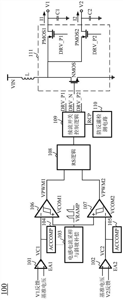
Multi-output boost circuit
A booster circuit, multi-output technology, applied in the direction of conversion equipment without intermediate conversion to AC, can solve the problems of high design difficulty, occupying chip area, and high circuit power consumption, saving circuit area cost, and being easy to design and implement. , to ensure the effect of normal continuous flow
- Summary
- Abstract
- Description
- Claims
- Application Information
AI Technical Summary
Problems solved by technology
Method used
Image


Examples
Embodiment Construction
[0049] In order to make the above objects, features and advantages of the present invention more comprehensible, specific implementations of the present invention will be described in detail below in conjunction with the accompanying drawings.
[0050] In the following description, many specific details are set forth in order to fully understand the present invention, but the present invention can also be implemented in other ways than those described here, so the present invention is not limited by the specific embodiments disclosed below.
[0051] As indicated in this application and claims, the terms "a", "an", "an" and / or "the" do not refer to the singular and may include the plural unless the context clearly indicates an exception. Generally speaking, the terms "comprising" and "comprising" only suggest the inclusion of clearly identified steps and elements, and these steps and elements do not constitute an exclusive list, and the method or device may also contain other step...
PUM
 Abstract
Description
Claims
Application Information