Synchronous acquisition processing card system based on multi-channel ADC and FPGA
A synchronous acquisition, multi-channel technology, applied in general control systems, control/regulation systems, instruments, etc., can solve the problem of inability to adapt to multi-channel synchronous high-speed high-precision acquisition and storage, poor signal processing and data processing capabilities, and small transmission bandwidth. and other issues, to achieve the effect of power consumption balance, wide data transmission bandwidth, and large number of channels
- Summary
- Abstract
- Description
- Claims
- Application Information
AI Technical Summary
Problems solved by technology
Method used
Image

Examples
Embodiment 1
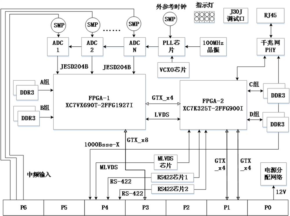
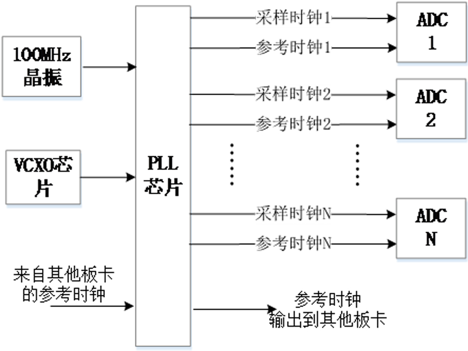
[0036] see figure 1 , a synchronous acquisition and processing card system based on multi-channel ADC and FPGA, including clock management unit, N pieces of ADC chips, two pieces of FPGA chips, four sets of DDR3 chips, power distribution network, N input from VPX connector P6 or P2 Analog IF signals are connected to multi-channel SMP access terminals through RF cables, coupled by front-end transformers, converted from single-ended signals to differential signals, and then input to the corresponding ADC chip. The sampling rate of the ADC chip is up to 14bit / 1000Msps AD9680BCPZ-1000 chip or 12bit / 2500Msps AD9625BBPZ-2.5 chip, multi-chip ADC chip sampling data is transmitted to FPGA1 through JESD204B protocol, FPGA1 uses Virtex-7 series XC7VX690T-2FFG1927I chip, and the synchronous reception of clock and data is completed in FPGA1; FPGA1 performs time-frequency analysis through FFT, and triggers data acquisition, storage and forwarding according to the level.
[0037] FPGA1 is c...
Embodiment 2
[0044] This embodiment is a further improvement made on the basis of the above embodiments, such as figure 1 As shown, in this embodiment, FPGA2 is externally connected with RS-422 / 485 interface chip, and RS-422 / 485 chip selects MAX3491 / MAX3485, and receives external input timing information or mutual communication information through RS-422 / 485 bus; Through MLVDS bus or RS-422 / 485 bus, long-distance data transmission or control is realized; FPGA2 is externally connected with a Gigabit network PHY chip, the chip model is 88E1111-B2-BAB1i000, and the PHY chip communicates with the RJ45 on the front panel of the board through GMII mode Connector connection for board debugging. The PHY chip is connected to the VPX connector through SGMII mode for external communication or debugging of this board.
[0045] This embodiment increases the MLVDS data transmission bus for communication between multiple boards, and the RS-422 / 485 data transmission bus for communication between devices, ...
Embodiment 3
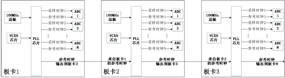
[0047] This embodiment is a further improvement made on the basis of the above embodiments, such as image 3 As shown, in this embodiment, board 1, board 2, and board 3 are synchronous acquisition and processing cards of three identical multi-channel ADCs and FPGAs in embodiment 1, and board 1 outputs 1 reference clock through the back The board is connected to the reference clock input terminal of the board card 2, and the reference clock output of the board card 2 is connected to the reference clock input terminal of the board card 3 through the backplane, thereby synchronizing the clocks of the three board cards, so that the board card 1 A total of 3×N sampling clocks and 3×N reference clocks of board 2 and board 3 have a stable phase synchronization relationship, so that the sampling data of 3×N ADCs of the three boards are synchronized, realizing Synchronous sampling of 3×N channels of data. Within the tolerance range of the cascaded clocks, synchronous sampling of more ...
PUM
 Abstract
Description
Claims
Application Information
 - R&D
- Intellectual Property
- Life Sciences
- Materials
- Tech Scout
- Unparalleled Data Quality
- Higher Quality Content
- 60% Fewer Hallucinations
Browse by: Latest US Patents, China's latest patents, Technical Efficacy Thesaurus, Application Domain, Technology Topic, Popular Technical Reports.
© 2025 PatSnap. All rights reserved.Legal|Privacy policy|Modern Slavery Act Transparency Statement|Sitemap|About US| Contact US: help@patsnap.com