Supercharge Your Innovation With Domain-Expert AI Agents!

Method for improving large layout efficiency of optical module PCB product

A technology for optical modules and products, which is used in measuring/indicating equipment, electrical components, and printed circuit manufacturing. The effect of efficiency

Pending Publication Date: 2020-10-16
BRAIN POWER (QING YUAN) CO LTD
View PDF0 Cites 0 Cited by
  • Summary
  • Abstract
  • Description
  • Claims
  • Application Information

AI Technical Summary

Problems solved by technology

The automatic production process is continuous production, and the output is large. Once there are factors that lead to product failure, but they are not found in time, it will lead to a batch of products that are not qualified and cause a lot of waste.
Some data show that in the automatic processing system, the downtime caused by milling cutter wear accounts for 20%-25% of the total number of failures, resulting in a reduction in production efficiency of more than 20%.

Method used


Image

  • Method for improving large layout efficiency of optical module PCB product
  • Method for improving large layout efficiency of optical module PCB product
  • Method for improving large layout efficiency of optical module PCB product

Examples


Embodiment Construction

[0017] The following will clearly and completely describe the technical solutions in the embodiments of the present invention with reference to the accompanying drawings in the embodiments of the present invention. Obviously, the described embodiments are only some, not all, embodiments of the present invention. Based on the embodiments of the present invention, all other embodiments obtained by persons of ordinary skill in the art without making creative efforts belong to the protection scope of the present invention.

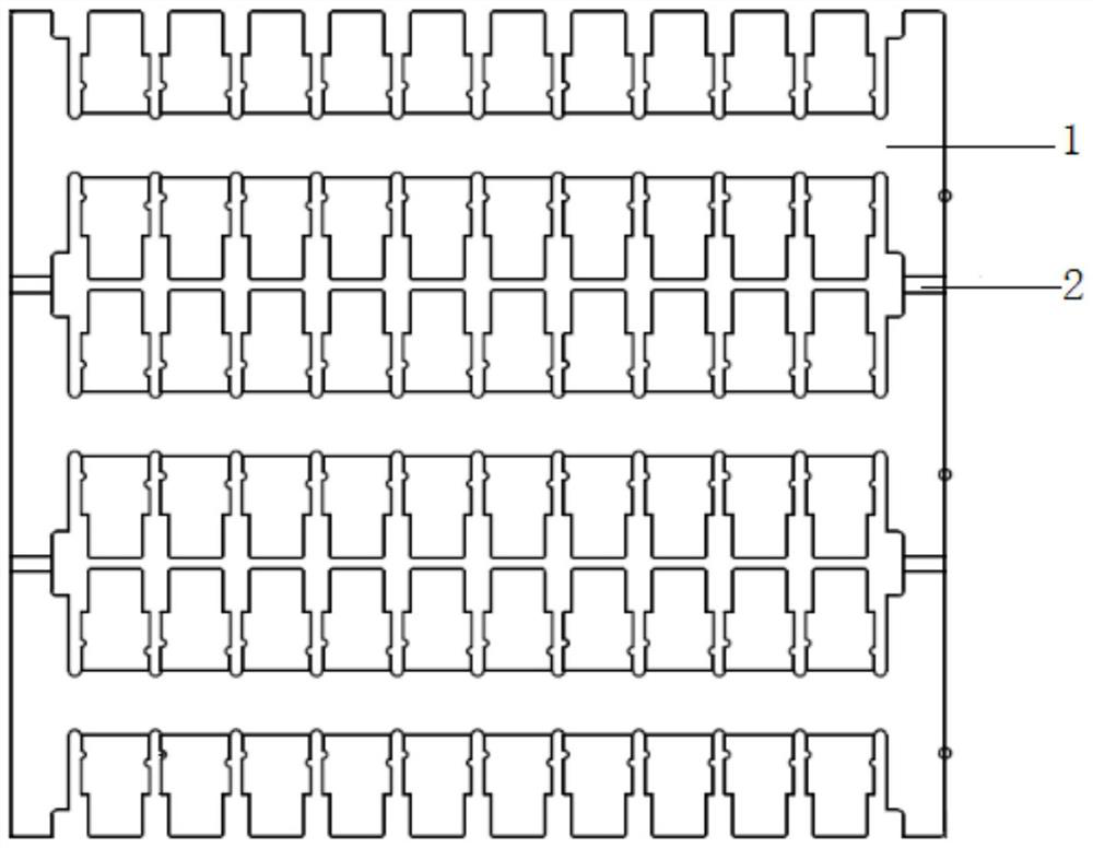
[0018] see Figure 1-5 , a method for improving the layout efficiency of optical module PCB products. The PCB product consists of 2-5 pieces connected together through the V-CUT groove. The depth of the V-CUT groove is 0.2-0.4mm, and the top angle of the V-CUT groove section The angle is 45°; the thickness of the single piece is 1.0mm; the surface processing accuracy of the single piece is micron level, and the surface roughness of the single piece is 0.3-0.5u...


PUM

PropertyMeasurementUnit
Thicknessaaaaaaaaaa
Surface roughnessaaaaaaaaaa

Abstract

The invention discloses a method for improving the large layout efficiency of an optical module PCB product, the PCB product is formed by connecting single chips through a V-CUT groove, the depth of the V-CUT groove is 0.2-0.4 mm, and the angle of the vertex angle of the cross section is 45 degrees; the automatic numerical control production process comprises a fixed-depth fishing and beveling program, an AVI program and an electric measurement jig program. According to the invention, V-CUT groove connection is realized between the single chips, the area of the PCB is increased, automatic or horizontal line cleaning is realized, and the production efficiency is improved; by arranging fixed-depth fishing and beveling program, the air suction, positioning, plate loading and unloading time issaved, and the production efficiency is improved by 50%; by arranging an electrical testing jig, the shutdown fault frequency and the number of defective products caused by abrasion of the milling cutter are reduced, and the production efficiency is improved; by setting the AVI program, defective products and rotating shaft damage caused by misalignment of the center line of the milling cutter and the center line of the rotating shaft can be monitored in real time, and then the production efficiency is improved.

Description

technical field [0001] The invention relates to the technical field of PCB product preparation, in particular to a method for improving the efficiency of large typesetting of optical module PCB products. Background technique [0002] The optical module PCB product is to fix the circuit components on the board. PCB products are small in size and easy to install. They are suitable for intelligent electronic components such as TVs, computers, and notebooks. The size of existing optical module PCB products is small, and the imposition size is also small. Because the board is too small, it cannot automatically pass through the horizontal cleaning line, so it can only be taped to pass through the horizontal line, resulting in low cleaning efficiency. During the production and processing of existing PCB boards, the precision and wear of milling cutters affect production efficiency. The machining accuracy of the milling cutter determines the tooth profile accuracy of the gear. Th...

Claims


Application Information

Patent Timeline
IPC IPC(8): H05K3/00B23Q17/09
CPCH05K3/0044H05K3/0055B23Q17/0957
Inventor 陈洁亮欧智鹏廖群良
Owner BRAIN POWER (QING YUAN) CO LTD
Features
  • R&D
  • Intellectual Property
  • Life Sciences
  • Materials
  • Tech Scout
  • Unparalleled Data Quality
  • Higher Quality Content
  • 60% Fewer Hallucinations
Learn More