Stepping exposure method based on UV-LED photoetching light source
A technology of UV-LED and exposure method, which is applied in the field of semiconductors and can solve the problem of limited exposure area
- Summary
- Abstract
- Description
- Claims
- Application Information
AI Technical Summary
Problems solved by technology
Method used
Image
Examples
Embodiment Construction
[0050] Embodiments of the present invention will be described below with reference to the accompanying drawings. Those skilled in the art would recognize that the described embodiments can be modified in various ways or combinations thereof without departing from the spirit and scope of the invention. Accordingly, the drawings and description are illustrative in nature and not intended to limit the scope of the claims. Also, in this specification, the drawings are not drawn to scale, and like reference numerals denote like parts.
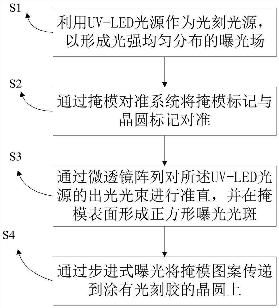
[0051] figure 1 It is a schematic flow chart of the step-by-step exposure method based on the UV-LED lithography light source of the present invention, as figure 1 As shown, the stepwise exposure method based on UV-LED lithography light source includes:
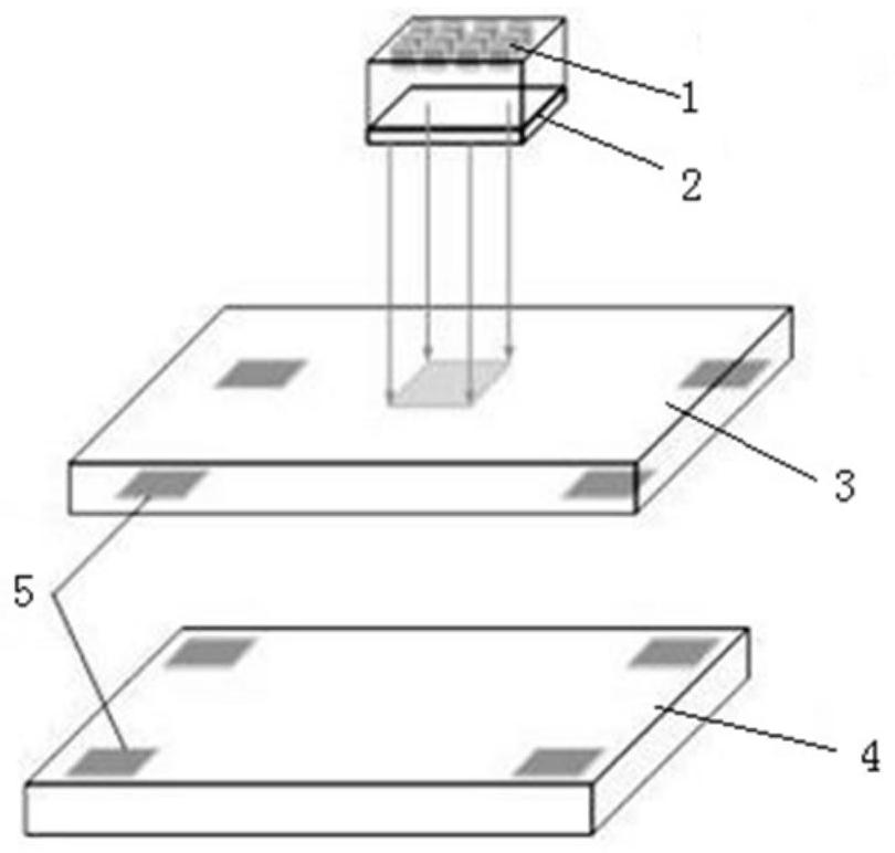
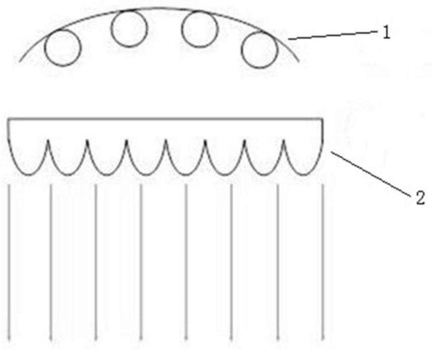
[0052] Step S1, using the UV-LED light source 1 as the lithography light source to form an exposure field with a uniform distribution of light intensity. The complex light source in the exposur...
PUM
 Abstract
Description
Claims
Application Information


