
Mask alignment photoetching machine based on UV-LED area array type light source

A UV-LED, mask alignment technology, applied in the semiconductor field, can solve the problems of complex light source collimation optical path, increased cost, increased structural complexity of lithography machine, etc.

Inactive Publication Date: 2020-10-20
BEIJING U PRECISION TECH
View PDF0 Cites 0 Cited by
  • Summary
  • Abstract
  • Description
  • Claims
  • Application Information

AI Technical Summary

Problems solved by technology

However, in general, the collimation optical path of the light source is relatively complicated, which increases the structural complexity of the lithography machine and leads to an increase in cost

Method used


Image

  • Mask alignment photoetching machine based on UV-LED area array type light source
  • Mask alignment photoetching machine based on UV-LED area array type light source
  • Mask alignment photoetching machine based on UV-LED area array type light source

Examples


Embodiment Construction

[0040] Embodiments of the present invention will be described below with reference to the accompanying drawings. Those skilled in the art would recognize that the described embodiments can be modified in various ways or combinations thereof without departing from the spirit and scope of the invention. Accordingly, the drawings and description are illustrative in nature and not intended to limit the scope of the claims. Also, in this specification, the drawings are not drawn to scale, and like reference numerals denote like parts.

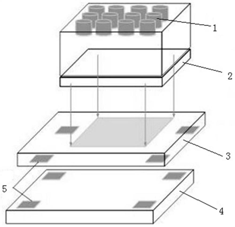
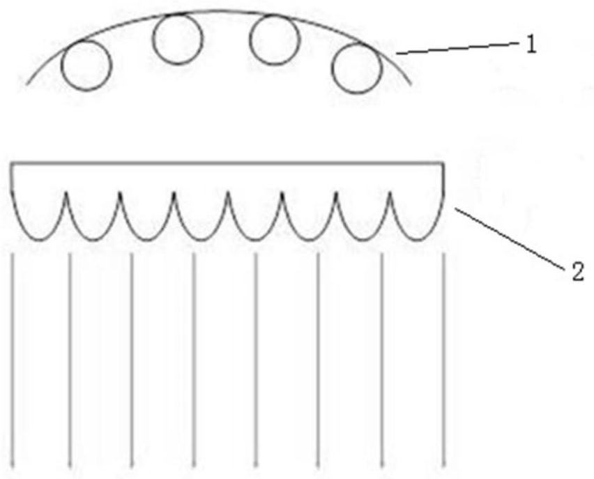
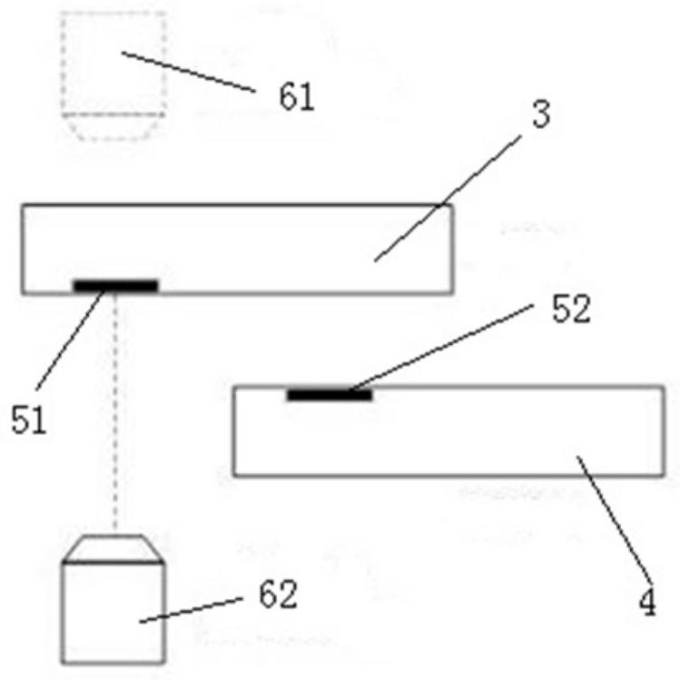
[0041] figure 1 is a structural schematic diagram of the mask alignment lithography machine of the present invention, figure 2 It is a schematic diagram of UV-LED light source and microlens array in the present invention, such as figure 1 with figure 2 As shown, the mask alignment lithography machine is a mask alignment lithography machine based on UV-LED area array light source, and its light source adopts UV-LED light source 1 to form an exp...


PUM


Abstract

The invention discloses a mask alignment photoetching machine based on a UV-LED area array type light source, and the mask alignment photoetching machine comprises a light source employing the UV-LEDlight source; a micro lens array, used for collimating an emergent light beam of the light source; a mask alignment system, used for aligning the mask mark with the wafer mark. The mask alignment system includes: a mask alignment system; a mechanical system, a control system and an image processing system, wherein the mechanical system comprises a mask workpiece table, a wafer workpiece table, a first driving mechanism and a second driving mechanism, the mask and the wafer are arranged in parallel, the control system is used for controlling the first driving mechanism and the second driving mechanism, and the image processing system is used for calibrating the overlap ratio of a mask mark and a wafer mark. An emergent light beam of the UV-LED light source forms a square exposure light spoton the surface of a mask through the micro lens array, and mask patterns are transmitted to a wafer through exposure. According to the invention, the submicron mask alignment precision can be realized, and a foundation is laid for realizing high-precision photoetching.

Description

technical field [0001] The present invention relates to the technical field of semiconductors, in particular to a mask alignment photolithography machine. Background technique [0002] Lithography machine is the basic device used in the field of semiconductor manufacturing technology and the core equipment for the production of large-scale integrated circuits. The development of lithography machines directly affects the development level of semiconductor manufacturing technology. In the existing lithography machine device, the light source is usually calibrated by using a light source collimation optical path, so as to improve the precision of the lithography machine. However, in general, the collimation optical path of the light source is relatively complicated, which increases the structural complexity of the photolithography machine, resulting in an increase in cost. Contents of the invention [0003] In view of the above problems, the object of the present invention ...

Claims


Application Information

Patent Timeline
IPC IPC(8): G03F7/20
CPCG03F7/2004G03F7/70075G03F7/70241G03F7/70725
Inventor 朱煜杨开明
Owner BEIJING U PRECISION TECH
Learn More