Heterojunction back contact solar cell and forming method thereof

A solar cell and heterojunction technology, applied in the field of solar cells, can solve the problems of complex patterning process and high battery cost

Inactive Publication Date: 2020-10-20
INST OF MICROELECTRONICS CHINESE ACAD OF SCI
View PDF7 Cites 3 Cited by
  • Summary
  • Abstract
  • Description
  • Claims
  • Application Information

AI Technical Summary

Problems solved by technology

[0005] In order to solve the problems of complex patterning process on the back of the conventional heterojunction back contact solar cell and

Method used


Image

  • Heterojunction back contact solar cell and forming method thereof
  • Heterojunction back contact solar cell and forming method thereof

Examples


Embodiment 1

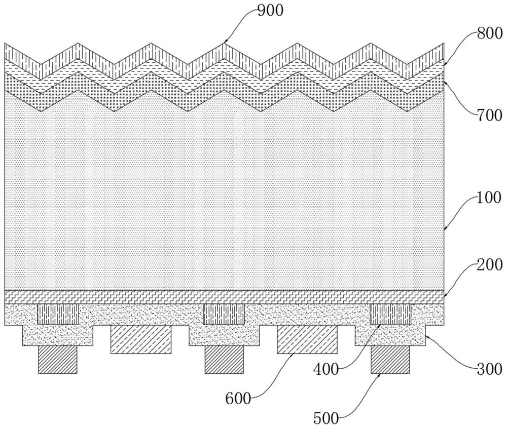
[0036] Such as figure 1 As shown, this embodiment can specifically provide a heterojunction back contact solar cell to solve at least one problem existing in the prior art. The heterojunction back contact solar cell may include but not limited to a semiconductor substrate 100, a first passivation layer 200, a P-type doped silicon film 300, an N-type doped silicon film 400, a first electrode 500 and a second electrode 600, front surface field 700, second passivation layer 800, anti-reflection layer 900 and so on.

[0037] The semiconductor substrate 100 has a front surface and a back surface. The front surface can be used to face the sun as a light-receiving surface to collect sunlight; the back surface can be used to place photovoltaic devices for photoelectric conversion. In some embodiments of the present invention, the front surface can be arranged facing upward, and a front surface composite layer is arranged on the front surface, and the front surface composite layer in...

Embodiment 2

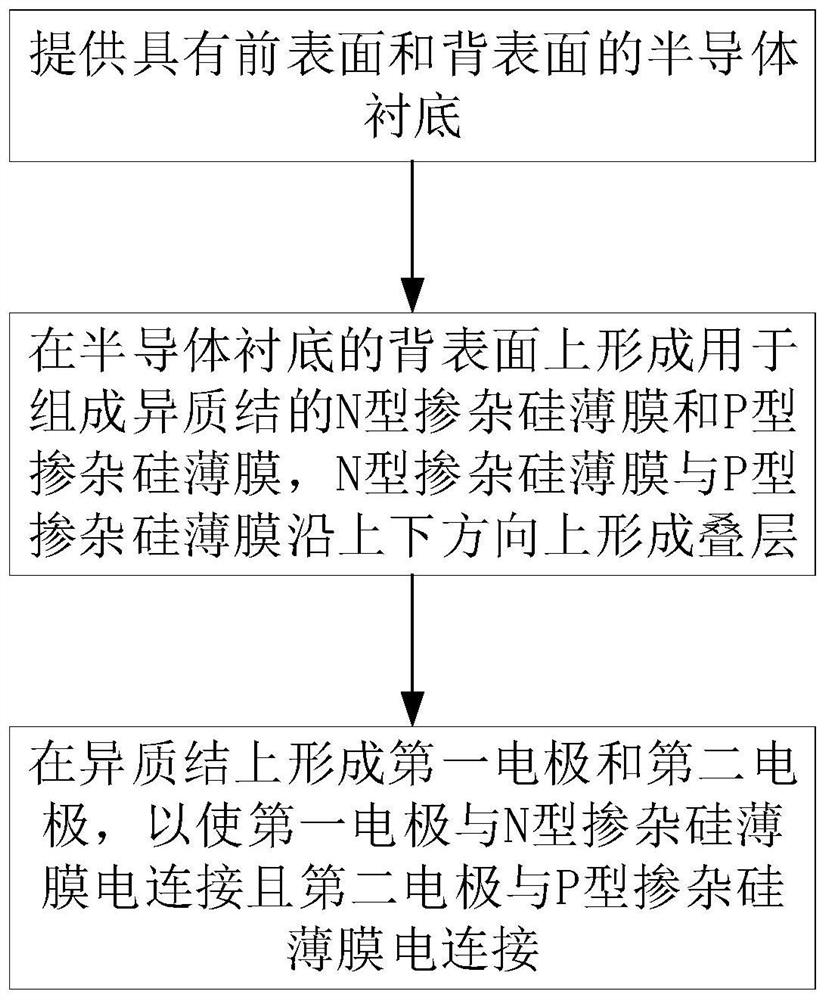
[0047] Based on the same inventive concept as the first embodiment, this embodiment provides a method for forming a heterojunction back contact solar cell, at least applicable to forming the structure of the heterojunction back contact solar cell in the first embodiment. By optimizing the growth process of the silicon thin film, the present invention can simplify the preparation process of the back pattern of the heterojunction back contact solar cell, and effectively reduce the preparation cost of the heterojunction back contact solar cell without reducing the conversion efficiency of the cell.

[0048] Such as figure 2 shown, and also see figure 1 , this embodiment provides a method for forming a heterojunction back contact solar cell, the method may include but not limited to the following steps.

[0049] A semiconductor substrate 100 is provided having a front surface and a back surface. The front surface is used to face the sun to collect sunlight; the back surface is ...


PUM

PropertyMeasurementUnit
Thicknessaaaaaaaaaa
Thicknessaaaaaaaaaa
Thicknessaaaaaaaaaa

Abstract

The invention discloses a heterojunction back contact solar cell and a forming method thereof. The heterojunction back contact solar cell comprises but is not limited to a semiconductor substrate, a first passivation layer and a heterojunction. The first passivation layer is formed on the back surface of the semiconductor substrate, the heterojunction can be formed on the back surface of the firstpassivation layer, the heterojunction comprises an N-type doped silicon thin film and a P-type doped silicon thin film, and the N-type doped silicon thin film and the P-type doped silicon thin film form a laminated structure along the vertical direction. The forming method of the heterojunction back contact solar cell comprises: forming a heterojunction on the back surface of a semiconductor substrate, the heterojunction comprising an N-type doped silicon thin film and a P-type doped silicon thin film which are formed in sequence, and the N-type doped silicon thin film and the P-type doped silicon thin film form a laminated layer in the vertical direction. According to the invention, the production cost of the heterojunction back contact solar cell can be effectively reduced on the premise that the cell efficiency is not reduced, and the light energy conversion efficiency is relatively high.

Description

technical field [0001] The present invention relates to the technical field of solar cells, and more specifically, the present invention relates to a heterojunction back contact solar cell and a forming method thereof. Background technique [0002] Crystalline silicon solar cells, as a device that can directly convert solar energy into electrical energy, have attracted more and more attention. Improving the conversion efficiency of crystalline silicon solar cells while reducing the production cost of the cells has always been the goal pursued by the industry and the key to improving its own competitiveness. [0003] Many scientific research institutions and enterprises at home and abroad have carried out a lot of research on high-efficiency crystalline silicon solar cells, and developed many high-efficiency crystalline silicon solar cells with new structures. These solar cell structures include grooved buried gate, selective emitter, crystalline silicon heterojunction (HIT,...

Claims


Application Information

Patent Timeline
IPC IPC(8): H01L31/0747H01L31/0224H01L31/0352H01L31/18
CPCH01L31/022441H01L31/0352H01L31/0747H01L31/1804Y02E10/547Y02P70/50
Inventor 陶科姜帅贾锐金智刘新宇
Owner INST OF MICROELECTRONICS CHINESE ACAD OF SCI
Why Eureka
Try Eureka