All-dielectric metasurface integrated Raman spectroscopy detection system

A detection system and Raman spectroscopy technology, which is applied in the field of all-dielectric metasurface integrated Raman spectroscopy detection system, can solve problems such as poor mechanical properties, inability to achieve synchronization, and no integration of Raman signals, so as to improve the high cost Effect

Active Publication Date: 2022-04-01
LASER FUSION RES CENT CHINA ACAD OF ENG PHYSICS
View PDF8 Cites 0 Cited by
  • Summary
  • Abstract
  • Description
  • Claims
  • Application Information

AI Technical Summary

Problems solved by technology

[0007] Strong surface plasmon resonance only occurs at the interface between substances with a negative dielectric constant and the medium. In the existing SERS sensing system, the plasma structure used to generate a strong electromagnetic field is made of noble metals. The cost of noble metals is high, and the mechanical Poor performance (possible oxidation, adhesion, poor adhesion) and other limitations
Most of the existing Raman sensing systems have prisms or metal grating structures for excitation and enhancement of Raman signals. In this form, the excitation and collection of Raman signals are carried out separately (excitation and collection of Raman signals) The collection is not integrated and cannot be synchronized)
This is a big obstacle to the realization of an integrated Raman spectroscopy detection system with a smaller integrated chip

Method used


Image

  • All-dielectric metasurface integrated Raman spectroscopy detection system
  • All-dielectric metasurface integrated Raman spectroscopy detection system
  • All-dielectric metasurface integrated Raman spectroscopy detection system

Examples


Embodiment Construction

[0025] The following will clearly and completely describe the technical solutions in the embodiments of the present invention with reference to the accompanying drawings in the embodiments of the present invention. Obviously, the described embodiments are only some, not all, embodiments of the present invention. Based on the embodiments of the present invention, all other embodiments obtained by persons of ordinary skill in the art without making creative efforts belong to the protection scope of the present invention.

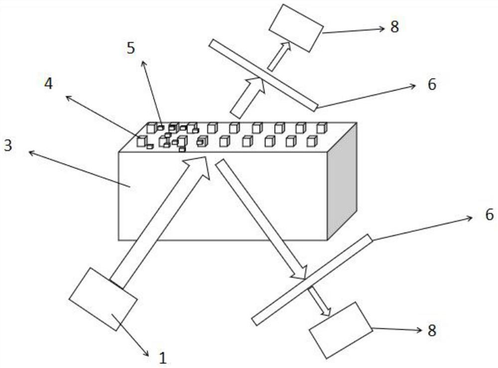
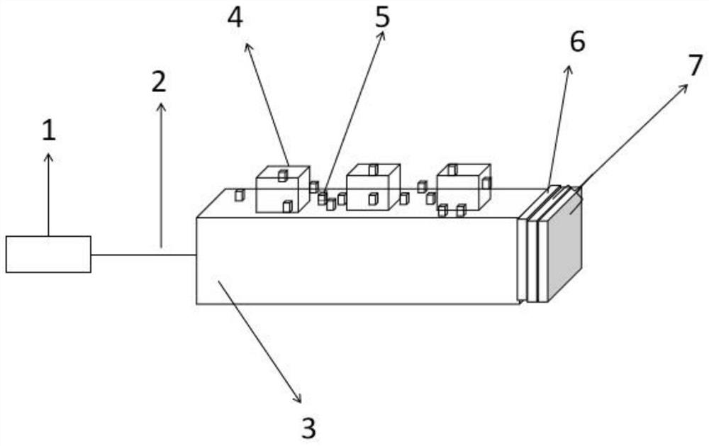
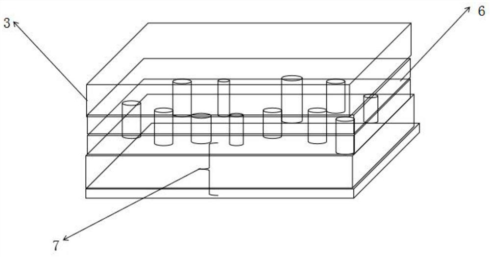
[0026] The main purpose of the present invention is to provide an all-dielectric metasurface integrated Raman spectroscopy detection system, improve the integration and intelligence of existing sensing systems, and improve the high cost and poor mechanical properties caused by the use of precious metal nanomaterials (possibly Oxidation, adhesion, poor adhesion) and other limitations. Realize the excitation, enhancement, and acquisition of Raman signals, which ...


PUM


Abstract

The invention relates to an all-dielectric metasurface integrated Raman spectrum detection system. The system includes a laser, an optical fiber, a waveguide, a nanostructure array, a filter and a metasurface spectrometer. The waveguide excites and transmits Raman signals. The nanostructure array is set on the upper surface of the waveguide. The nanostructure array provides a strong electromagnetic field to suspend the probe molecules. Around the nanostructure array, the probe molecules emit Raman signals under the action of a strong electromagnetic field. The filter is plated at the output end of the waveguide, and the filter filters out the pump light output by the waveguide. The metasurface chip spectrometer is set on the surface of the filter. The metasurface chip spectrometer analyzes the Raman signal after the filter filters out the incident light band, and obtains various spectral information of the detected molecule. The invention can realize the excitation, enhancement and acquisition of Raman signals synchronously on the same structure, and complete the goal of a highly integrated chip-based Raman sensing system.

Description

technical field [0001] The invention relates to the field of Raman spectrum detection, in particular to an all-dielectric metasurface integrated Raman spectrum detection system. Background technique [0002] Raman scattering is a kind of inelastic scattering, which is caused by the exchange of incident photon and molecular energy in the interaction between light and matter. Therefore, different molecules and even different chemical bonds have different Raman peak positions, and have non-destructive properties. The unique advantage of being intrusive and non-identifying. Raman spectroscopy has gradually developed into a mature technique for analyzing chemistry and biomolecules in many applications such as pharmacology and food safety. However, it has the disadvantage of low signal intensity, the intensity of conventional Raman signal is only 10 of the incident light intensity. -6 —10 -12 , it is very difficult to detect the Raman signal, and it is usually necessary to enha...

Claims


Application Information

Patent Timeline
Patent Type & Authority Patents(China)
IPC IPC(8): G01N21/65
CPCG01N21/658
Inventor 叶鑫唐烽陈骏李波杨李茗邵婷孙来喜李青芝石兆华
Owner LASER FUSION RES CENT CHINA ACAD OF ENG PHYSICS
Why Eureka
Try Eureka