

Semiconductor structure and forming method thereof
一种半导体、图形结构的技术,应用在半导体器件、半导体/固态器件制造、电固体器件等方向,能够解决性能有待提升等问题
- Summary
- Abstract
- Description
- Claims
- Application Information
AI Technical Summary
Problems solved by technology
Method used
Image

Examples
Embodiment Construction
[0027] As mentioned in the background, the performance of the fin field effect transistor formed by the prior art needs to be improved. The structure of a fin field effect transistor is now described and analyzed.
[0028] Figure 1 to Figure 3 It is a schematic cross-sectional structure diagram of a formation process of an embodiment of a semiconductor structure.
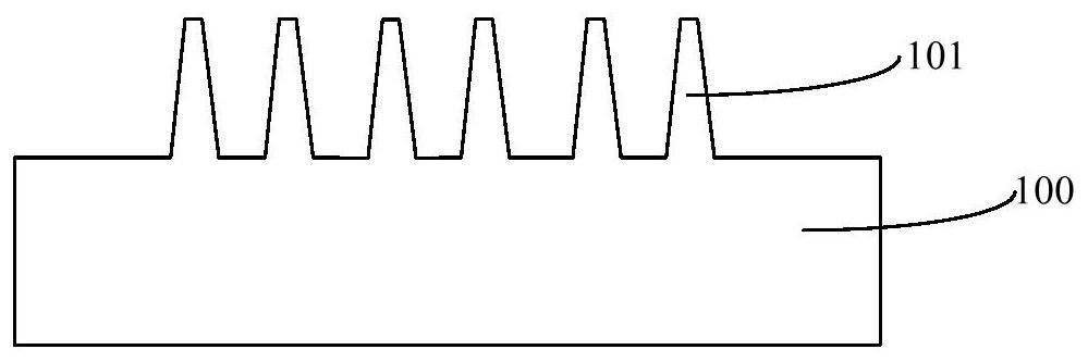
[0029] Please refer to figure 1 , providing a base 100 with fins 101 on the base, and the fins 101 are separated from each other on the substrate 100 .
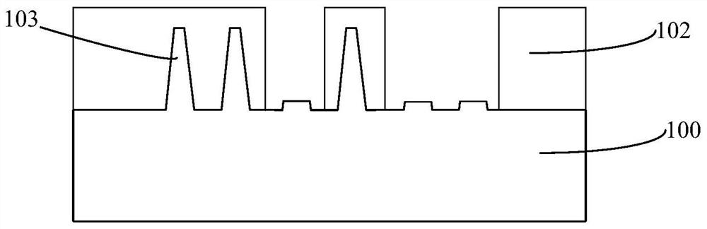
[0030] Please refer to figure 2 A mask layer 102 is formed on the substrate 100 and the fins 101 , the mask layer 102 exposes part of the fins 101 ; part of the fins 101 is removed to form a target fin 103 .
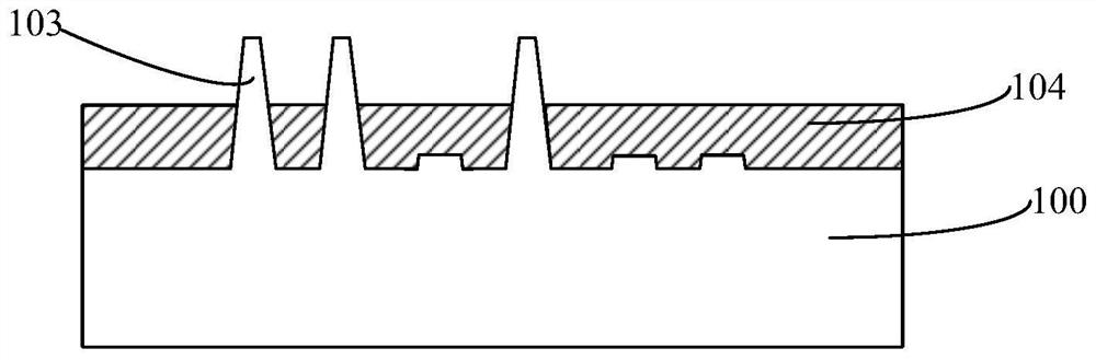
[0031] Please refer to image 3 After the target fin 103 is formed, the mask layer 102 is removed, and an isolation structure 104 is formed on the substrate 100 , the isolation structure 104 covers part of the sidewall of the target fin 103 and is lowe...
PUM
 Abstract
Description
Claims
Application Information